REV. A
Information furnished by Analog Devices is believed to be accurate and
reliable. However, no responsibility is assumed by Analog Devices for its
use, nor for any infringements of patents or other rights of third parties that
may result from its use. No license is granted by implication or otherwise
under any patent or patent rights of Analog Devices.
a
OP27
One Technology Way, P.O. Box 9106, Norwood, MA 02062-9106, U.S.A.
Tel: 781/329-4700 www.analog.com
Fax: 781/326-8703 © Analog Devices, Inc., 2002
Low-Noise, Precision
Operational Amplifier
PIN CONNECTIONS
TO-99
(J-Suffix)
V+
OUT
NC
4V– (CASE)
BAL
BAL 1
–IN 2
+IN 3
OP27
NC = NO CONNECT
FEATURES
Low Noise: 80 nV p-p (0.1 Hz to 10 Hz), 3 nV/
√
Hz
Low Drift: 0.2 V/C
High Speed: 2.8 V/s Slew Rate, 8 MHz Gain
Bandwidth
Low V
OS
: 10 V
Excellent CMRR: 126 dB at V
CM
of ±11 V
High Open-Loop Gain: 1.8 Million
Fits 725, OP07, 5534A Sockets
Available in Die Form
GENERAL DESCRIPTION
The OP27 precision operational amplifier combines the low
offset and drift of the OP07 with both high speed and low noise.
Offsets down to 25 µV and drift of 0.6 µV/°C maximum make
the OP27 ideal for precision instrumentation applications.
Exceptionally low noise, e
n
= 3.5 nV/√Hz, at 10 Hz, a low 1/f
noise corner frequency of 2.7 Hz, and high gain (1.8 million),
allow accurate high-gain amplification of low-level signals. A
gain-bandwidth product of 8 MHz and a 2.8 V/µsec slew rate
provides excellent dynamic accuracy in high-speed, data-
acquisition systems.
A low input bias current of ± 10 nA is achieved by use of a
bias-current-cancellation circuit. Over the military temperature
range, this circuit typically holds I
B
and I
OS
to ±20 nA and 15 nA,
respectively.
The output stage has good load driving capability. A guaranteed
swing of ±10 V into 600 Ω and low output distortion make the
OP27 an excellent choice for professional audio applications.
(Continued on page 7)
V–
V+
Q2B
R2*
Q3
Q2AQ1A Q1B
R4
R1*
R3
18
V
OS
ADJ.
R1 AND R2 ARE PERMANENTLY
ADJUSTED AT WAFER TEST FOR
MINIMUM OFFSET VOLTAGE.
*
NONINVERTING
INPUT (+)
INVERTING
INPUT (–)
Q6
Q21
C2
R23 R24
Q23
Q24
Q22
R5
Q11 Q12
Q27 Q28
C1
R9
R12
C3 C4
Q26
Q20 Q19
Q46
Q45
OUTPUT
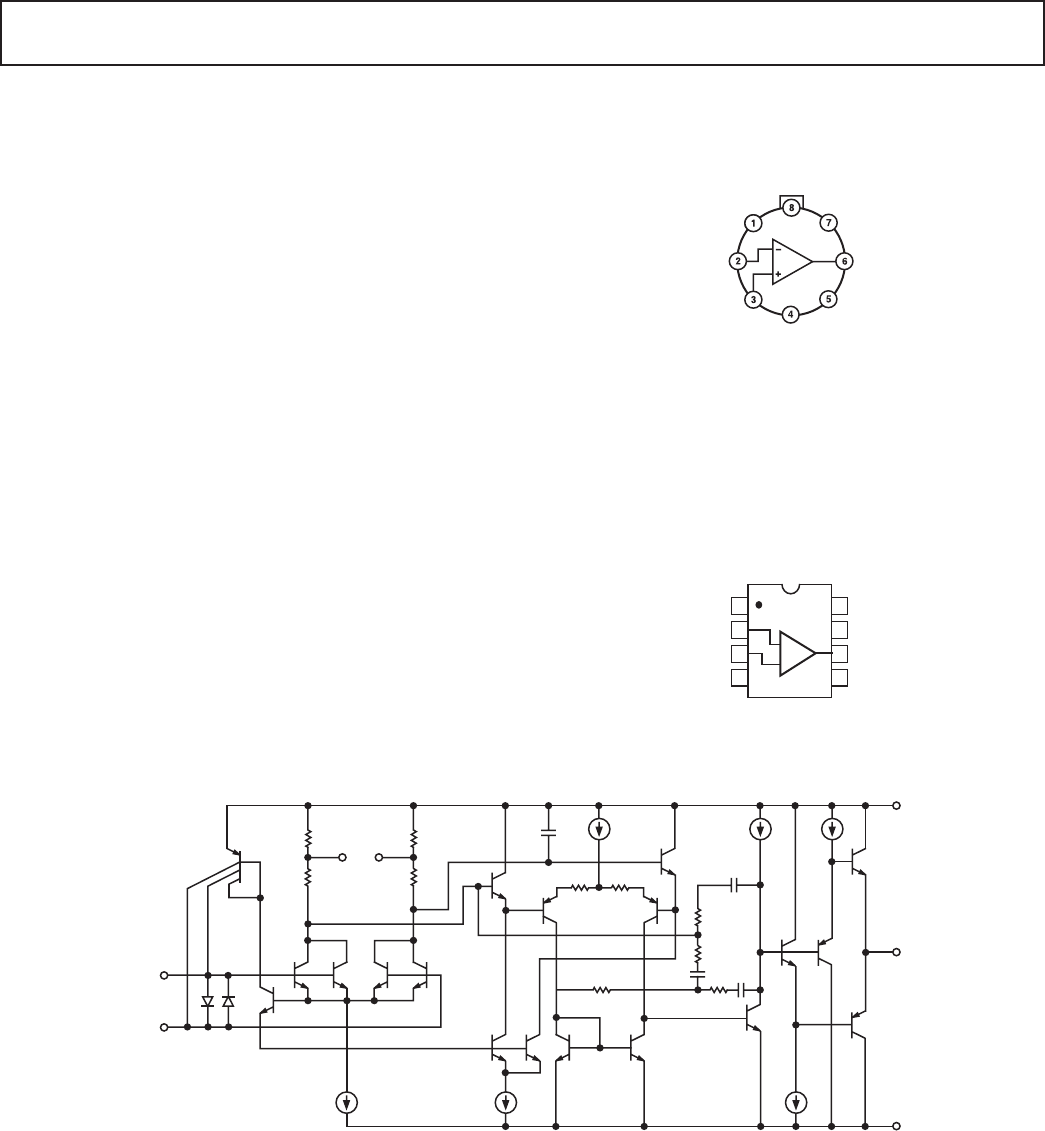
Figure 1. Simplified Schematic
8-Pin Hermetic DIP
(Z-Suffix)
Epoxy Mini-DIP
(P-Suffix)
8-Pin SO
(S-Suffix)
8
7
6
5
1
2
3
4
NC = NO CONNECT
V
OS
TRIM
–IN
+IN
V
OS
TRIM
V+
OUT
NCV–
OP27


