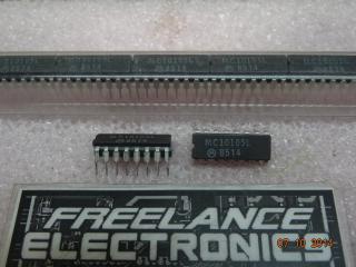
Freelance Electronics Components Distributor
Closed Dec 25th-26th
800-300-1968
We Stock Hard to Find Parts

MC10198L

Part # MC10198L
Description Monostable Multivibrator Single 16-Pin CDIP
Category Microcircuit
Availability In Stock
Qty 1
Qty Price
1 + $10.85673
Manufacturer Available Qty
Motorola Corp
Date Code: 8028
  • Shipping Freelance Stock: 1
    Ships Immediately


Technical Document


DISCLAIMER: The information provided herein is solely for informational purposes. Customers must be aware of the suitability of this product for their application, and consider that variable factors such as Manufacturer, Product Category, Date Codes, Pictures and Descriptions may differ from available inventory.

Semiconductor Components Industries, LLC, 2002
January, 2002 – Rev. 7
1 Publication Order Number:
MC10198/D
MC10198
Monostable Multivibrator
The MC10198 is a retriggerable monostable multivibrator. Two
enable inputs permit triggering on any combination of positive or
negative edges as shown in the accompanying table. The trigger input
is buffered by Schmitt triggers making it insensitive to input rise and
fall times.
The pulse width is controlled by an external capacitor and resistor.
The resistor sets a current which is the linear discharge rate of the
capacitor. Also, the pulse width can be controlled by an external
current source or voltage (see applications information).
For high–speed response with minimum delay, a hi–speed input is
also provided. This input bypasses the internal Schmitt triggers and the
output responds within 2 nanoseconds typically.
Output logic and threshold levels are standard MECL 10,000. Test
conditions are per Table 2. Each “Precondition” referred to in Table 2
is per the sequence of Table 1.
P
D
= 415 mW typ/pkg (No Load)
t
pd
= 4.0 ns typ Trigger Input to Q
2.0 ns typ Hi–Speed Input to Q
Min Timing Pulse Width PW
Qmin
10 ns typ
1
Max Timing Pulse Width PW
Qmax
>10 ms typ
2
Min Trigger Pulse Width PW
T
2.0 ns typ
Min Hi–Speed PW
HS
3.0 ns typ
Trigger Pulse Width
Enable Setup Time t
set
1.0 ns typ
Enable Hold Time t
hold
1.0 ns typ
1
C
Ext
= 0 (Pin 4 open), R
Ext
= 0
(Pin 6 to V
EE
)
2
C
Ext
= 10 mF, R
Ext
= 2.7 kW
http://onsemi.com
Device Package Shipping
ORDERING INFORMATION
MC10198L CDIP–16 25 Units / Rail
MC10198P PDIP–16 25 Units / Rail
MC10198FN PLCC–20 46 Units / Rail
MARKING
DIAGRAMS
1
16
A = Assembly Location
WL = Wafer Lot
YY = Year
WW = Work Week
CDIP–16
L SUFFIX
CASE 620
MC10198L
AWLYYWW
PDIP–16
P SUFFIX
CASE 648
PLCC–20
FN SUFFIX
CASE 775
10198
AWLYYWW
1
1
16
MC10198P
AWLYYWW
MC10198
http://onsemi.com
2
DIP
PIN ASSIGNMENT
V
CC1
Q
Q
C
EXT
E
POS
R
EXT
EXT.PULSE
WIDTH CONTROL
V
EE
V
CC2
HIGH-SPEED
INPUT
N/C
TRIGGER INPUT
N/C
N/C
E
NEG
N/C
16
15
14
13
12
11
10
9
1
2
3
4
5
6
7
8
Pin assignment is for Dual–in–Line Package.
For PLCC pin assignment, see the Pin Conversion Tables on page 18
of the ON Semiconductor MECL Data Book (DL122/D).
LOGIC DIAGRAM
V
CC1
= PIN 1
V
CC2
= PIN 16
V
EE
= PIN 8
5
7
10
13
15
3
2
Q
Q
64
V
EE
V
CC
C
EXT
E pos
EXTERNAL PULSE
WIDTH CONTROL
E
NEG
TRIGGER
INPUT
HI-SPEED
INPUT
TRUTH TABLE
E
Pos
E
Neg
L
L
H
H
INPUT
OUTPUT
L
H
L
H
Triggers on both positive & negative input slopes
Triggers on positive input slope
Triggers on negative input slope
Trigger is disabled
R
EXT
1. At t = 0 a.) Apply V
IHmax
to Pin 5 and 10.
b.) Apply V
ILmin
to Pin 15.
c.) Ground Pin 4.
2. At t 10 ns a.) Open Pin 1.
b.) Apply –3.0 Vdc to Pin 4.
Hold these conditions for
10 ns.
3. Return Pin 4 to Ground and perform test as
indicated in Table 2.
Pins 1, 16 = V
CC
= Ground
Pins 6, 8 = V
EE
= –5.2 Vdc
Outputs loaded 50 to –2.0 Vdc
V
IH
max
V
IL
min
P1
-5.0
0
10 ns
t(ns)
-4.0
-3.0
-2.0
-1.0
0(Gnd)
10 20
Pin 1
open
30
TABLE 1 — PRECONDITION SEQUENCE
Pin 4 Voltage (Vdc)
10 ns
TABLE 2 — CONDITIONS FOR TESTING OUTPUT LEVELS
(See Table 1 for Precondition Sequence)
V
ILA
max
V
IL
min
P2
V
IHA
max
V
IL
min
P3
MC10198
http://onsemi.com
3
Pin Conditions Pin Conditions
Test P.U.T. 5 10 13 15 Test P.U.T. 5 10 13 15
Precondition Precondition
V
OH
2 V
IL
min
V
OHA
2 V
IHA
min
P1
V
OH
3 P1 V
OHA
3 V
ILA
max
P1
Precondition Precondition
V
OL
3 V
IL
min
V
OLA
3 V
ILA
max
V
OL
2 P1 V
OLA
2 V
IHA
min
Precondition Precondition
V
OHA
2 V
ILA
max
V
OLA
2 V
IL
min
V
OHA
3 V
IHA
min
V
OLA
3 V
IL
min
Precondition Precondition
V
OHA
2 V
IL
min
V
OLA
3 P2
V
OHA
3 P3 V
OLA
2 P3
Precondition Precondition
V
OHA
2 P2 V
OLA
3 V
IH
max
P2
V
OHA
3 P3 V
OLA
2 V
IH
max
P3
Precondition Precondition
V
OHA
2 V
IH
max
P2 V
OLA
3V
IHA
min
V
IH
max
P1
V
OHA
3 V
IH
max
P3 V
OLA
2V
ILA
max
V
IH
max
P1
Precondition Precondition
V
OHA
2 V
IH
max
P1 V
OLA
3V
IH
max
V
IHA
min
P1
V
OHA
3 V
IH
max
P1 V
OLA
2V
IH
max
V
ILA
max
P1
1234NEXT