Closed Dec 25th-26th
800-300-1968
We Stock Hard to Find Parts
My Account
|
My Orders
|
My Cart
Questions?
(800) 300-1968
Register
(current)
My Account
(current)
My Orders
(current)
My Cart
(current)
Categories
(current)
Manufacturers
Request a Quote
Sell Your Excess
Consignment
Quality Assurance
3000
Part #
3000
Description
DUP RCPT PORTABLE OUTLET BX
Category
LED
Availability
Out of Stock
Qty
0
Qty
Price
1 +
$0.15000
Related Items
Generic
LED
3000
$0.15000
SCHURTER
LED
0035.0727
$10.81417
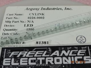
ARGOSY INDUSRTIES INC.
LED
0226-0002
$0.27485
LEDTRONICS
LED
0286A5442P0A43
LEDTRONICS
LED
0286A5442P0A52
LEDTRONICS
LED
0286A5442P0A53