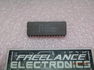
Freelance Electronics Components Distributor
Closed Dec 25th-26th
800-300-1968
We Stock Hard to Find Parts

5962-9087001MLA

Part # 5962-9087001MLA
Description Bus XCVR Single 8-CH 3-ST 24-Pin CDIP Tube - Rail/Tube
Category IC
Availability In Stock
Qty 6
Qty Price
1 - 1 $32.93997
2 - 2 $26.20225
3 - 3 $24.70497
4 - 5 $22.95816
6 + $20.46271
Manufacturer Available Qty
Texas Instruments
  • Shipping Freelance Stock: 6
    Ships Immediately


Technical Document


DISCLAIMER: The information provided herein is solely for informational purposes. Customers must be aware of the suitability of this product for their application, and consider that variable factors such as Manufacturer, Product Category, Date Codes, Pictures and Descriptions may differ from available inventory.

SN54BCT543, SN74BCT543
OCTAL REGISTERED TRANSCEIVERS
WITH 3-STATE OUTPUTS
SCBS026C – NOVEMBER 1988 – REVISED APRIL 1994
Copyright 1994, Texas Instruments Incorporated
2–1
POST OFFICE BOX 655303 DALLAS, TEXAS 75265
State-of-the-Art BiCMOS Design
Significantly Reduces I
CCZ
3-State True Outputs
Back-to-Back Registers for Storage
ESD Protection Exceeds 2000 V
Per MIL-STD-883C, Method 3015
Package Options Include Plastic
Small-Outline Packages (DW), Ceramic
Chip Carriers (FK) and Flatpacks (W), and
Plastic and Ceramic 300-mil DIPs (JT, NT)
description
The BCT543 octal transceiver contains two sets
of D-type latches for temporary storage of data
flowing in either direction. Separate latch-enable
(LEAB
or LEBA) and output-enable (OEAB or
OEBA) inputs are provided for each register to
permit independent control in either direction of
data flow.
The A-to-B enable (CEAB) input must be low in
order to enter data from A or to output data from
B. If CEAB is low and LEAB is low, the A-to-B
latches are transparent; a subsequent low-to-high
transition of LEAB
puts the A latches in the storage
mode. With CEAB and OEAB both low, the 3-state
B outputs are active and reflect the data present
at the output of the A latches. Data flow from B to
A is similar but requires using the CEBA
, LEBA,
and OEBA inputs.
The SN54BCT543 is characterized for operation
over the full military temperature range of –55°C
to 125°C. The SN74BCT543 is characterized for
operation from 0°C to 70°C.
FUNCTION TABLE
INPUTS
OUTPUT
CEAB LEAB OEAB A
B
H X X X Z
X XHX Z
L HLX B
0
L LLL L
L L L H H
A-to-B data flow is shown; B-to-A flow control is the
same except that it uses CEBA
, LEBA, and OEBA.
Output level before the indicated steady-state input
conditions were established.
SN54BCT543 . . . JT OR W PACKAGE
SN74BCT543 . . . DW OR NT PACKAGE
(TOP VIEW)
1
2
3
4
5
6
7
8
9
10
11
12
24
23
22
21
20
19
18
17
16
15
14
13
LEBA
OEBA
A1
A2
A3
A4
A5
A6
A7
A8
CEAB
GND
V
CC
CEBA
B1
B2
B3
B4
B5
B6
B7
B8
LEAB
OEAB
SN54BCT543 . . . FK PACKAGE
(TOP VIEW)
3212827
12 13
5
6
7
8
9
10
11
25
24
23
22
21
20
19
B2
B3
B4
NC
B5
B6
B7
A2
A3
A4
NC
A5
A6
A7
426
14 15 16 1718
A8
CEAB
GND
NC
OEAB
LEAB
B8
A1
OEBA
LEBA
NC
CEBA
B1
V
CC
NC – No internal connection
PRODUCTION DATA information is current as of publication date.
Products conform to specifications per the terms of Texas Instruments
standard warranty. Production processing does not necessarily include
testing of all parameters.
SN54BCT543, SN74BCT543
OCTAL REGISTERED TRANSCEIVERS
WITH 3-STATE OUTPUTS
SCBS026C – NOVEMBER 1988 – REVISED APRIL 1994
2–2
POST OFFICE BOX 655303 DALLAS, TEXAS 75265
logic symbol
1
1
4
2C6
14
3
A1
4
A2
B1
22
5D
5
A3
6
A4
7
A5
8
A6
9
A7
10
A8
B2
21
B3
20
B5
18
B4
19
B6
17
B8
15
B7
16
LEAB
3
G2
11
CEAB
2EN4
13
OEAB
1C5
1
LEBA
G1
23
CEBA
1EN3
2
OEBA
6D
This symbol is in accordance with ANSI/IEEE Std 91-1984 and IEC Publication 617-12.
logic diagram (positive logic)
OEBA
CEBA
LEBA
OEAB
CEAB
LEAB
A1
B1
C1
1D
C1
1D
2
23
1
13
11
14
3
22
To Seven Other Channels
Pin numbers shown are for the DW, JT, NT, and W packages.
SN54BCT543, SN74BCT543
OCTAL REGISTERED TRANSCEIVERS
WITH 3-STATE OUTPUTS
SCBS026C – NOVEMBER 1988 – REVISED APRIL 1994
2–3
POST OFFICE BOX 655303 DALLAS, TEXAS 75265
absolute maximum ratings over operating free-air temperature range (unless otherwise noted)
Supply voltage range, V
CC
– 0.5 V to 7 V. . . . . . . . . . . . . . . . . . . . . . . . . . . . . . . . . . . . . . . . . . . . . . . . . . . . . . . . . .
Input voltage range: Control inputs (see Note 1) – 0.5 V to 7 V. . . . . . . . . . . . . . . . . . . . . . . . . . . . . . . . . . . . . . . .
I/O ports (see Note 1) – 0.5 V to 5.5 V. . . . . . . . . . . . . . . . . . . . . . . . . . . . . . . . . . . . . . . . . .
Voltage range applied to any output in the disabled or power-off state, V
O
– 0.5 V to 7 V. . . . . . . . . . . . . . . . .
Voltage range applied to any output in the high state, V
O
– 0.5 V to V
CC
. . . . . . . . . . . . . . . . . . . . . . . . . . . . . . .
Input clamp current, I
IK
–30 mA. . . . . . . . . . . . . . . . . . . . . . . . . . . . . . . . . . . . . . . . . . . . . . . . . . . . . . . . . . . . . . . . . .
Current into any output in the low state: SN54BCT543 96 mA. . . . . . . . . . . . . . . . . . . . . . . . . . . . . . . . . . . . . . . .
SN74BCT543 128 mA. . . . . . . . . . . . . . . . . . . . . . . . . . . . . . . . . . . . . . .
Operating free-air temperature range: SN54BCT543 – 55°C to 125°C. . . . . . . . . . . . . . . . . . . . . . . . . . . . . . . .
SN74BCT543 0°C to 70°C. . . . . . . . . . . . . . . . . . . . . . . . . . . . . . . . . . . .
Storage temperature range – 65°C to 150°C. . . . . . . . . . . . . . . . . . . . . . . . . . . . . . . . . . . . . . . . . . . . . . . . . . . . . . . .
Stresses beyond those listed under “absolute maximum ratings” may cause permanent damage to the device. These are stress ratings only, and
functional operation of the device at these or any other conditions beyond those indicated under “recommended operating conditions” is not
implied. Exposure to absolute-maximum-rated conditions for extended periods may affect device reliability.
NOTE 1: The input and output voltage ratings may be exceeded if the input and output current ratings are observed.
recommended operating conditions
SN54BCT543 SN74BCT543
UNIT
MIN NOM MAX MIN NOM MAX
UNIT
V
CC
Supply voltage 4.5 5 5.5 4.5 5 5.5 V
V
IH
High-level input voltage 2 2 V
V
IL
Low-level input voltage 0.8 0.8 V
I
IK
Input clamp current –18 –18 mA
I
OH
High-level output current –12 –15 mA
I
OL
Low-level output current 48 64 mA
T
A
Operating free-air temperature –55 125 0 70 °C
12345NEXT