Freelance Electronics Components Distributor
Closed Dec 25th-26th
800-300-1968
We Stock Hard to Find Parts

5962-8982401PA

Part # 5962-8982401PA
Description IC MONO 5V REFERENCE IC
Category IC
Availability In Stock
Qty 2
Qty Price
1 + $25.88509
Manufacturer Available Qty
Analog Devices
Date Code: 0043
  • Shipping Freelance Stock: 2
    Ships Immediately


Technical Document


DISCLAIMER: The information provided herein is solely for informational purposes. Customers must be aware of the suitability of this product for their application, and consider that variable factors such as Manufacturer, Product Category, Date Codes, Pictures and Descriptions may differ from available inventory.

AD586
Rev. G | Page 4 of 16
AD586M, AD586S, AD586T
@ T
A
= 25°C, V
IN
= 15 V, unless otherwise noted. Specifications in boldface are tested on all production units at final electrical test. Results
from those tests are used to calculate outgoing quality levels. All minimum and maximum specifications are guaranteed, although only
those shown in boldface are tested on all production units, unless otherwise specified.
Table 2.
AD586M AD586S AD586T
Parameter Min Typ Max Min Typ Max Min Typ Max Unit
OUTPUT VOLTAGE 4.998 5.002 4.990 5.010 4.9975 5.0025 V
OUTPUT VOLTAGE
DRIFT
1
0°C to 70°C 2 ppm/°C
−55°C to +125°C 20 10 ppm/°C
GAIN ADJUSTMENT
+6
+6
+6
%
−2 −2 −2 %
LINE REGULATION
1
10.8 V < +V
IN
< 36 V
T
MIN
to T
MAX
±100
µV/V
11.4 V < +V
IN
< 36 V
T
MIN
to T
MAX
±150
±150
µV/V
LOAD REGULATION
1
Sourcing 0 mA < I
OUT
< 10 mA
25°C
100
150
150
µV/mA
T
MIN
to T
MAX
100
150
150
µV/mA
Sinking −10 mA < I
OUT
< 0 mA
25°C
400 400 400 µV/mA
QUIESCENT CURRENT 2
3
2
3
2
3
mA
POWER CONSUMPTION 30 30 30 mW
OUTPUT NOISE
0.1 Hz to 10 Hz 4 4 4 µV p-p
Spectral Density,
100 Hz
100 100 100 nV/√Hz
LONG-TERM STABILITY 15 15 15 ppm/1000 hr
SHORT-CIRCUIT
CURRENT-TO-GROUND
45
60
45
60
45
60
mA
TEMPERATURE RANGE
Specified Performance
2
0 70 −55 +125 −55 +125 °C
Operating Performance
3
−40 +85 −55 +125 −55 +125 °C
1
Maximum output voltage drift is guaranteed for all packages and grades. CERDIP packaged parts are also 100°C production tested.
2
Lower row shows specified performance for A and B grades.
3
The operating temperature range is defined as the temperature extremes at which the device will still function. Parts may deviate from their specified performance
outside their specified temperature range.
AD586
Rev. G | Page 5 of 16
ABSOLUTE MAXIMUM RATINGS
Table 3.
Parameter Rating
V
IN
to Ground 36 V
Power Dissipation (25°C) 500 mW
Storage Temperature −65°C to +150°C
Lead Temperature (Soldering, 10 sec) 300°C
Package Thermal Resistance
θ
JC
22°C/W
θ
JA
110°C/W
Output Protection
Output safe for indefinite
short to ground or V
IN
.
Stresses above those listed under Absolute Maximum Ratings
may cause permanent damage to the device. This is a stress
rating only; functional operation of the device at these or any
other conditions above those indicated in the operational
section of this specification is not implied. Exposure to absolute
maximum rating conditions for extended periods may affect
device reliability.
ESD CAUTION
ESD (electrostatic discharge) sensitive device. Electrostatic charges as high as 4000 V readily accumulate on the
human body and test equipment and can discharge without detection. Although this product features
proprietary ESD protection circuitry, permanent damage may occur on devices subjected to high energy
electrostatic discharges. Therefore, proper ESD precautions are recommended to avoid performance
degradation or loss of functionality.
AD586
Rev. G | Page 6 of 16
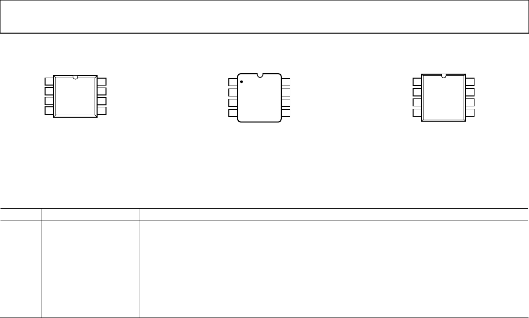
PIN CONFIGURATIONS AND FUNCTION DESCRIPTIONS
1
TP DENOTES FACTORY TEST POINT.
NO CONNECTIONS, EXCEPT DUMMY PCB PAD,
SHOULD BE MADE TO THESE POINTS.
TP
1
1
V
IN
2
TP
1
3
GND
4
NOISE
REDUCTION
8
TP
1
7
V
OUT
6
TRIM
5
AD586
TOP VIEW
(Not to Scale)
00529-002
Figure 2. Pin Configuration (N-8)
1
TP DENOTES FACTORY TEST POINT.
NO CONNECTIONS, EXCEPT DUMMY PCB PAD,
SHOULD BE MADE TO THESE POINTS.
00529-003
TP
1
1
V
IN
2
TP
1
3
GND
4
NOISE
REDUCTION
8
TP
1
7
V
OUT
6
TRIM
5
AD586
TOP VIEW
(Not to Scale)
Figure 3. Pin Configuration (Q-8)
1
TP DENOTES FACTORY TEST POINT.
NO CONNECTIONS, EXCEPT DUMMY PCB PAD,
SHOULD BE MADE TO THESE POINTS.
00529-004
TP
1
1
V
IN
2
TP
1
3
GND
4
NOISE
REDUCTION
8
TP
1
7
V
OUT
6
TRIM
5
AD586
TOP VIEW
(Not to Scale)
Figure 4. Pin Configuration (R-8)
Table 4. Pin Function Descriptions
Pin No. Mnemonic Description
1 TP
1
Factory Trim Pad (No Connect).
2 V
IN
Input Voltage.
3 TP
1
Factory Trim Pad (No Connect).
4 GND Ground.
5 TRIM Optional External Fine Trim. See the Applying the AD586 section.
6 V
OUT
Output Voltage.
7 TP
1
Factory Trim Pad (No Connect).
8 NOICE REDUCTION Optional Noise Reduction Filter with External 1µF Capacitor to Ground.
PREVIOUS123456NEXT