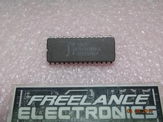
STANDARD
SIZE
A
5962-88630
COLUMBUS, OHIO 43218-3990
REVISION LEVEL
G
SHEET
3
DSCC FORM 2234
APR 97
1.2.4 Case outline(s). The case outline(s) are as designated in MIL-STD-1835 and as follows:
Outline letter Descriptive designator Terminals Package style
K GDFP2-F24 or CDFP3-F24 24 Flat pack
V GDIP1-T18 or CDIP2-T18 18 Dual-in-line
3 CQCC1-N28 28 Square leadless chip carrier
1.2.5 Lead finish. The lead finish is as specified in MIL-PRF-38535 for device classes Q and V or MIL-PRF-38535,
appendix A for device class M.
1.3 Absolute maximum ratings. 1/
Supply voltage (V
S
) ..................................................................................... ±18 V dc
Power dissipation (P
D
) ................................................................................ 500 mW 2/
Common mode input voltage ...................................................................... Supply voltage
Differential input voltage:
R
G
≥ 2 kΩ ................................................................................................ ±20 V dc
R
G
< 2 kΩ ................................................................................................ ±10 V dc
Output short circuit duration ........................................................................ Indefinite
Storage temperature range ......................................................................... -65°C to +150°C
Lead temperature (soldering, 60 seconds) .................................................. +300°C
Thermal resistance, junction-to-case (θ
JC
) ................................................. See MIL-STD-1835
Thermal resistance, junction-to-ambient (θ
JA
):
Case V ..................................................................................................... 120°C/W
Case 3 ...................................................................................................... 104°C/W
Case K ..................................................................................................... 69°C/W
1.4 Recommended operating conditions.
Supply voltage (V
S
) ..................................................................................... ±15 V dc
Ambient operating temperature range (T
A
) ................................................. -55°C to +125°C
______
1/ Stresses above the absolute maximum rating may cause permanent damage to the device. Extended operation at the
maximum levels may degrade performance and affect reliability.
2/ Must withstand the added P
D
due to short circuit test, e.g., I
OS
.