Closed Dec 25th-26th
800-300-1968
We Stock Hard to Find Parts
My Account
|
My Orders
|
My Cart
Questions?
(800) 300-1968
Register
(current)
My Account
(current)
My Orders
(current)
My Cart
(current)
Categories
(current)
Manufacturers
Request a Quote
Sell Your Excess
Consignment
Quality Assurance
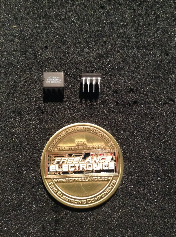
5962-8859301MPA
Part #
5962-8859301MPA
Description
DUAL LOW-OFFSET/POWER IC500KHZ DUAL 8CERDIP
Category
IC
Availability
Out of Stock
Qty
0
Qty
Price
1 +
$20.75036
Related Items
AMI
IC
5962-00A0801QXC
AMIS
IC
5962-05A0101NXB
Atmel
IC
5962-3826701MXA
$235.60318
Atmel
IC
5962-3826707MXA
$243.51752
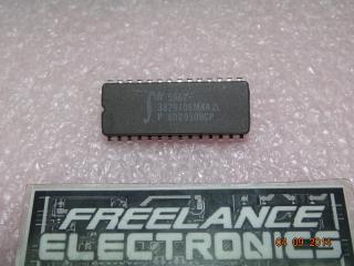
Integrated Device Technology
IC
5962-3829406MXA
$24.80000
LOGIC DEVICES INCORPORATED
IC
5962-3829409MUA
$71.87469