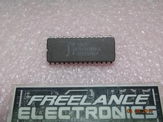
Freelance Electronics Components Distributor
Closed Dec 25th-26th
800-300-1968
We Stock Hard to Find Parts

5962-8759401XA

Part # 5962-8759401XA
Description IC, MICROPOWER VOLTAGE REFERE - Rail/Tube
Category IC
Availability In Stock
Qty 1106
Qty Price
1 - 9 $25.48585
10 - 24 $20.27283
25 - 52 $19.11439
53 - 112 $17.76286
113 + $15.83212
Manufacturer Available Qty
  • Shipping Freelance Stock: 16
    Ships Immediately
Linear Technology
Date Code: 9521
  • Shipping Freelance Stock: 10
    Ships Immediately
Linear Technology
Date Code: 9500
  • Shipping Freelance Stock: 2
    Ships Immediately
Linear Technology
Date Code: 9232
  • Shipping Freelance Stock: 1075
    Ships Immediately
National Semiconductor Corp
Date Code: 0648
  • Shipping Freelance Stock: 3
    Ships Immediately


Technical Document


DISCLAIMER: The information provided herein is solely for informational purposes. Customers must be aware of the suitability of this product for their application, and consider that variable factors such as Manufacturer, Product Category, Date Codes, Pictures and Descriptions may differ from available inventory.

LM185-1.2QML
www.ti.com
SNVS384B OCTOBER 2005REVISED JANUARY 2014
LM185-1.2QML Micropower Voltage Reference Diode
Check for Samples: LM185-1.2QML
1
FEATURES
DESCRIPTION
The LM185-1.2 is a micropower 2-terminal band-gap
2
Operating Current of 10μA to 20mA
voltage regulator diodes. Operating over a 10μA to
1Ω Maximum Dynamic Impedance (Typical)
20mA current range, it features exceptionally low
Low Temperature Coefficient
dynamic impedance and good temperature stability.
On-chip trimming is used to provide tight voltage
Radiation Qualified Option
tolerance. Since the LM185-1.2 band-gap reference
100 krad
uses only transistors and resistors, low noise and
Low Dose Rate Tested at 10 mrad/s
good long term stability result.
Careful design of the LM185-1.2 has made the device
exceptionally tolerant of capacitive loading, making it
easy to use in almost any reference application. The
wide dynamic operating range allows its use with
widely varying supplies with excellent regulation.
The extremely low power drain of the LM185-1.2
makes it useful for micropower circuitry. This voltage
reference can be used to make portable meters,
regulators or general purpose analog circuitry with
battery life approaching shelf life.
Further, the wide operating current allows it to
replace older references with a tighter tolerance part.
Connection Diagrams
Figure 1. LCCC Package Figure 2. TO Package Bottom View
See Package Number NAJ0020A See Package Number NDU0002A
1
Please be aware that an important notice concerning availability, standard warranty, and use in critical applications of
Texas Instruments semiconductor products and disclaimers thereto appears at the end of this data sheet.
2All trademarks are the property of their respective owners.
PRODUCTION DATA information is current as of publication date.
Copyright © 2005–2014, Texas Instruments Incorporated
Products conform to specifications per the terms of the Texas
Instruments standard warranty. Production processing does not
necessarily include testing of all parameters.
1
2
3
4
10
9
8
7
5 6
+V
REF
NC
NC
NC
NC
NC
NC
NC
NC
V-
LM185-1.2QML
SNVS384B OCTOBER 2005REVISED JANUARY 2014
www.ti.com
Figure 3. CLGA Package
See Package Number NAC0010A
Schematic Diagram
These devices have limited built-in ESD protection. The leads should be shorted together or the device placed in conductive foam
during storage or handling to prevent electrostatic damage to the MOS gates.
2 Submit Documentation Feedback Copyright © 2005–2014, Texas Instruments Incorporated
Product Folder Links: LM185-1.2QML
LM185-1.2QML
www.ti.com
SNVS384B OCTOBER 2005REVISED JANUARY 2014
Absolute Maximum Ratings
(1)
Reverse Current 30mA
Forward Current 10mA
Operating Temperature Range 55°C T
A
+125°C
Maximum Junction Temperature (T
Jmax
)
(2)
+150°C
Storage Temperature 55°C T
A
+150°C
Lead Temperature (Soldering 10 CLGA 260°C
Seconds)
TO package 300°C
20LD LCCC package 300°C
Thermal Resistance θ
JA
TO (Still Air) 300°C/W
TO (500LF / Min Air Flow) 139°C/W
20LD LCCC (Still Air) 100°C/W
20LD LCCC (500LF / Min Air 73°C/W
Flow)
CLGA (Still Air) 194°C/W
CLGA (500LF / Min Air Flow) 128°C/W
θ
JC
TO 57°C/W
20LD LCCC 25°C/W
CLGA 23°C/W
Package Weight (Typical) TO TBD
20LD LCCC TBD
CLGA 210mg
ESD Tolerance
(3)
4KV
(1) Absolute Maximum Ratings indicate limits beyond which damage to the device may occur. Operating Ratings indicate conditions for
which the device is functional. For specifications and test conditions, see the Electrical Characteristics. The specifications apply only for
the test conditions listed. Some performance characteristics may degrade when the device is not operated under the listed test
conditions.
(2) The maximum power dissipation must be derated at elevated temperatures and is dictated by T
Jmax
(maximum junction temperature),
θ
JA
(package junction to ambient thermal resistance), and T
A
(ambient temperature). The maximum allowable power dissipation at any
temperature is P
Dmax
= (T
Jmax
- T
A
)/θ
JA
or the number given in the Absolute Maximum Ratings, whichever is lower.
(3) Human body model, 1.5K in series with 100pF.
Quality Conformance Inspection
Table 1. Mil-Std-883, Method 5005 - Group A
Subgroup Description Temp °C
1 Static tests at 25
2 Static tests at 125
3 Static tests at -55
4 Dynamic tests at 25
5 Dynamic tests at 125
6 Dynamic tests at -55
7 Functional tests at 25
8A Functional tests at 125
8B Functional tests at -55
9 Switching tests at 25
10 Switching tests at 125
11 Switching tests at -55
12 Settling time at 25
13 Settling time at 125
14 Settling time at -55
Copyright © 2005–2014, Texas Instruments Incorporated Submit Documentation Feedback 3
Product Folder Links: LM185-1.2QML
123456NEXT