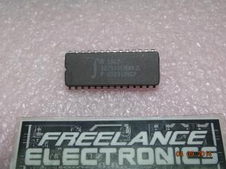
Freelance Electronics Components Distributor
Closed Dec 25th-26th
800-300-1968
We Stock Hard to Find Parts

5962-8682601EA

Part # 5962-8682601EA
Description Shift Register Single 4-Bit Serial/Parallel to Parallel 16
Category IC
Availability In Stock
Qty 17
Qty Price
1 - 3 $15.62336
4 - 7 $12.42767
8 - 10 $11.71752
11 - 14 $10.88901
15 + $9.70542
Manufacturer Available Qty
Harris Corporation
Date Code: 9401
  • Shipping Freelance Stock: 17
    Ships Immediately


Technical Document


DISCLAIMER: The information provided herein is solely for informational purposes. Customers must be aware of the suitability of this product for their application, and consider that variable factors such as Manufacturer, Product Category, Date Codes, Pictures and Descriptions may differ from available inventory.

1
Data sheet acquired from Harris Semiconductor
SCHS164G
Features
Four Operating Modes
- Shift Right, Shift Left, Hold and Reset
Synchronous Parallel or Serial Operation
Typical f
MAX
= 60MHz at V
CC
= 5V, C
L
= 15pF,
T
A
= 25
o
C
Asynchronous Master Reset
Fanout (Over Temperature Range)
- Standard Outputs. . . . . . . . . . . . . . . 10 LSTTL Loads
- Bus Driver Outputs . . . . . . . . . . . . . 15 LSTTL Loads
Wide Operating Temperature Range . . . -55
o
C to 125
o
C
Balanced Propagation Delay and Transition Times
Significant Power Reduction Compared to LSTTL
Logic ICs
HC Types
- 2V to 6V Operation
- High Noise Immunity: N
IL
= 30%, N
IH
= 30% of V
CC
at V
CC
= 5V
HCT Types
- 4.5V to 5.5V Operation
- Direct LSTTL Input Logic Compatibility,
V
IL
= 0.8V (Max), V
IH
= 2V (Min)
- CMOS Input Compatibility, I
l
1µA at V
OL
, V
OH
Pinout
CD54HC194 (CERDIP)
CD74HC194 (PDIP, SOIC, SOP, TSSOP)
CD74HCT194 (PDIP)
TOP VIEW
Description
The ’HC194 and CD74HCT194 are 4-bit shift registers with
Asynchronous Master Reset (
MR). In the parallel mode (S0
and S1 are high), data is loaded into the associated flip-flop
and appears at the output after the positive transition of the
clock input (CP). During parallel loading serial data flow is
inhibited. Shift left and shift right are accomplished
synchronously on the positive clock edge with serial data
entered at the shift left (DSL) serial input for the shift left
mode, and at the shift right (DSR) serial input for the shift
right mode. Clearing the register is accomplished by a Low
applied to the Master Reset (
MR) pin.
14
15
16
9
13
12
11
10
1
2
3
4
5
7
6
8
MR
DSR
D
0
D
1
D
2
D
3
GND
DSL
V
CC
Q
1
Q
2
Q
3
CP
S1
S0
Q
0
Ordering Information
PART NUMBER
TEMP. RANGE
(
o
C) PACKAGE
CD54HC194F3A -55 to 125 16 Ld CERDIP
CD74HC194E -55 to 125 16 Ld PDIP
CD74HC194M -55 to 125 16 Ld SOIC
CD74HC194MT -55 to 125 16 Ld SOIC
CD74HC194M96 -55 to 125 16 Ld SOIC
CD74HC194NSR -55 to 125 16 Ld SOP
CD74HC194PW -55 to 125 16 Ld TSSOP
CD74HC194PWR -55 to 125 16 Ld TSSOP
CD74HC194PWT -55 to 125 16 Ld TSSOP
CD74HCT194E -55 to 125 16 Ld PDIP
NOTE: When ordering, use the entire part number. The suffixes 96
and R denote tape and reel. The suffix T denotes a small-quantity
reel of 250.
September 1997 - Revised May 2006
CAUTION: These devices are sensitive to electrostatic discharge. Users should follow proper IC Handling Procedures.
Copyright
© 2006, Texas Instruments Incorporated
CD54HC194, CD74HC194,
CD74HCT194
High-Speed CMOS Logic
4-Bit Bidirectional Universal Shift Register
[
/Title
(
CD74
H
C194,
C
D74H
C
T194)
/
Sub-
j
ect
(
High-
S
peed
C
MOS
L
ogic
4
-Bit
2
Functional Diagram
TRUTH TABLE
OPERATING
MODE
INPUTS OUTPUT
CP MR S1 S0 DSR DSL D
n
Q
0
Q
1
Q
2
Q
3
Reset (Clear) X L X X X X X LLLL
Hold (Do Nothing) X H l l X X X q
0
q
1
q
2
q
3
Shift Left H h l XlXq
1
q
2
q
3
L
Hh l XhXq
1
q
2
q
3
H
Shift Right Hl hlXXLq
0
q
1
q
2
Hl hhXXHq
0
q
1
q
2
Parallel Load Hh hXXd
n
d
0
d
1
d
2
d
3
H = High Voltage Level,
h = High Voltage Level One Set-up Time Prior To The Low to High Clock Transition,
L = Low Voltage Level,
l = Low Voltage Level One Set-up Time Prior to the Low to High Clock Transition,
d
n
(q
n
) = Lower Case Letters Indicate the State of the Referenced Input (or output) One Set-up Time Prior to the Low To High Clock
Transition,
X = Don’t Care,
= Transition from Low to High Level
14
12
13
15
Q
0
Q
1
Q
2
Q
3
7
6
3
4
5
D
0
D
1
D
2
D
3
GND = 8
V
CC
= 16
2 9 10 1 11
DSL
DSR
S0
S1
MR
CP
CD54HC194, CD74HC194, CD74HCT194
3
Absolute Maximum Ratings Thermal Information
DC Supply Voltage, V
CC
. . . . . . . . . . . . . . . . . . . . . . . . -0.5V to 7V
DC Input Diode Current, I
IK
For V
I
< -0.5V or V
I
> V
CC
+ 0.5V. . . . . . . . . . . . . . . . . . . . . .±20mA
DC Output Diode Current, I
OK
For V
O
< -0.5V or V
O
> V
CC
+ 0.5V . . . . . . . . . . . . . . . . . . . .±20mA
DC Output Source or Sink Current per Output Pin, I
O
For V
O
> -0.5V or V
O
< V
CC
+ 0.5V . . . . . . . . . . . . . . . . . . . .±25mA
DC V
CC
or Ground Current, I
CC or
I
GND
. . . . . . . . . . . . . . . . . .±50mA
Operating Conditions
Temperature Range (T
A
) . . . . . . . . . . . . . . . . . . . . . -55
o
C to 125
o
C
Supply Voltage Range, V
CC
HC Types . . . . . . . . . . . . . . . . . . . . . . . . . . . . . . . . . . . . .2V to 6V
HCT Types . . . . . . . . . . . . . . . . . . . . . . . . . . . . . . . . .4.5V to 5.5V
DC Input or Output Voltage, V
I
, V
O
. . . . . . . . . . . . . . . . . 0V to V
CC
Input Rise and Fall Time
2V . . . . . . . . . . . . . . . . . . . . . . . . . . . . . . . . . . . . . . 1000ns (Max)
4.5V. . . . . . . . . . . . . . . . . . . . . . . . . . . . . . . . . . . . . . 500ns (Max)
6V . . . . . . . . . . . . . . . . . . . . . . . . . . . . . . . . . . . . . . . 400ns (Max)
Package Thermal Impedance, θ
JA
(see Note 2):
E (PDIP) Package . . . . . . . . . . . . . . . . . . . . . . . . . . . . . . .67
o
C/W
M (SOIC) Package. . . . . . . . . . . . . . . . . . . . . . . . . . . . . . .73
o
C/W
NS (SOP) Package . . . . . . . . . . . . . . . . . . . . . . . . . . . . . 64
o
C/W
PW (TSSOP) Package . . . . . . . . . . . . . . . . . . . . . . . . . 108
o
C/W
Maximum Junction Temperature . . . . . . . . . . . . . . . . . . . . . . . 150
o
C
Maximum Storage Temperature Range . . . . . . . . . .-65
o
C to 150
o
C
Maximum Lead Temperature (Soldering 10s) . . . . . . . . . . . . . 300
o
C
(SOIC - Lead Tips Only)
CAUTION: Stresses above those listed in “Absolute Maximum Ratings” may cause permanent damage to the device. This is a stress only rating and operation
of the device at these or any other conditions above those indicated in the operational sections of this specification is not implied.
NOTE:
1. The package thermal impedance is calculated in accordance with JESD 51-7.
DC Electrical Specifications
PARAMETER SYMBOL
TEST
CONDITIONS
V
CC
(V)
25
o
C -40
o
C TO 85
o
C -55
o
C TO 125
o
C
UNITSV
I
(V) I
O
(mA) MIN TYP MAX MIN MAX MIN MAX
HC TYPES
High Level Input
Voltage
V
IH
- - 2 1.5 - - 1.5 - 1.5 - V
4.5 3.15 - - 3.15 - 3.15 - V
6 4.2 - - 4.2 - 4.2 - V
Low Level Input
Voltage
V
IL
- - 2 - - 0.5 - 0.5 - 0.5 V
4.5 - - 1.35 - 1.35 - 1.35 V
6 - - 1.8 - 1.8 - 1.8 V
High Level Output
Voltage
CMOS Loads
V
OH
V
IH
or
V
IL
-0.02 2 1.9 - - 1.9 - 1.9 - V
-0.02 4.5 4.4 - - 4.4 - 4.4 - V
-0.02 6 5.9 - - 5.9 - 5.9 - V
High Level Output
Voltage
TTL Loads
-4 4.5 3.98 - - 3.84 - 3.7 - V
-5.2 6 5.48 - - 5.34 - 5.2 - V
Low Level Output
Voltage
CMOS Loads
V
OL
V
IH
or
V
IL
0.02 2 - - 0.1 - 0.1 - 0.1 V
0.02 4.5 - - 0.1 - 0.1 - 0.1 V
0.02 6 - - 0.1 - 0.1 - 0.1 V
Low Level Output
Voltage
TTL Loads
4 4.5 - - 0.26 - 0.33 - 0.4 V
5.2 6 - - 0.26 - 0.33 - 0.4 V
CD54HC194, CD74HC194, CD74HCT194
12345NEXT