Closed Dec 25th-26th
800-300-1968
We Stock Hard to Find Parts
My Account
|
My Orders
|
My Cart
Questions?
(800) 300-1968
Register
(current)
My Account
(current)
My Orders
(current)
My Cart
(current)
Categories
(current)
Manufacturers
Request a Quote
Sell Your Excess
Consignment
Quality Assurance
54LS155DMQB
Part #
54LS155DMQB
Description
Category
IC
Availability
In Stock
Qty
2
Qty
Price
1 +
$2.61782
Manufacturer
Available
Qty
Fairchild Semiconductor
Freelance Stock:
2
Ships Immediately
Add to Cart
Related Items
Texas Instruments
IC
54LS10/BCAJC
$9.91653
SIGNETICS
IC
54LS109/BEA
$9.91653
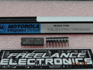
Motorola Corp
IC
54LS109A/YBDGAQ2
$5.00000
Fairchild Semiconductor
IC
54LS10DM
$4.37563
Fairchild Semiconductor
IC
54LS10DMQB
$0.32179
Fairchild Semiconductor
IC
54LS10DMQB/C
$7.51252