Closed Dec 25th-26th
800-300-1968
We Stock Hard to Find Parts
My Account
|
My Orders
|
My Cart
Questions?
(800) 300-1968
Register
(current)
My Account
(current)
My Orders
(current)
My Cart
(current)
Categories
(current)
Manufacturers
Request a Quote
Sell Your Excess
Consignment
Quality Assurance
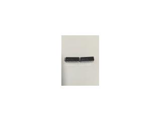
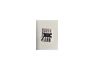
54F374FK
Part #
54F374FK
Description
Category
IC
Availability
Out of Stock
Qty
0
Qty
Price
1 +
$12.60000
Related Items
SIGNETICS
IC
54F373/BRA
$28.92990
Motorola Corp
IC
54F373/BRAJC
$15.34159
Fairchild Semiconductor
IC
54F373DMQB
$18.65977
National Semiconductor Corp
IC
54F373DMQB/QS
$15.34159
Fairchild Semiconductor
IC
54F373DMQBW
$9.54188
NAT/FAIR
IC
54F373FMQB
$14.85069