Closed Dec 25th-26th
800-300-1968
We Stock Hard to Find Parts
My Account
|
My Orders
|
My Cart
Questions?
(800) 300-1968
Register
(current)
My Account
(current)
My Orders
(current)
My Cart
(current)
Categories
(current)
Manufacturers
Request a Quote
Sell Your Excess
Consignment
Quality Assurance
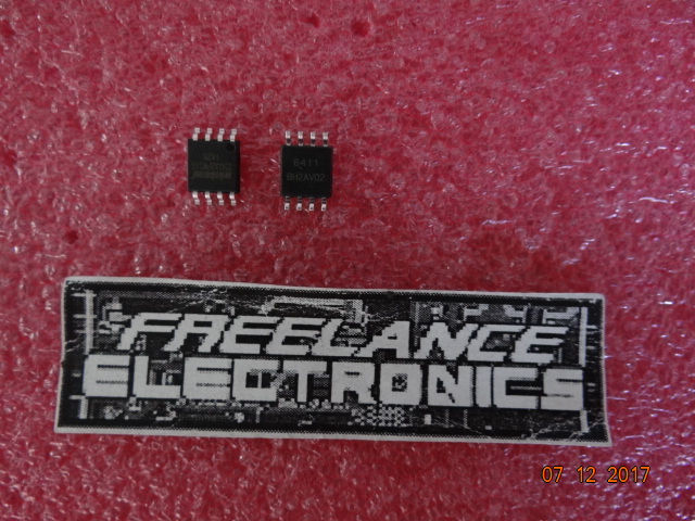
W25Q32FWSSIG
Part #
W25Q32FWSSIG
Description
NOR Flash Serial (SPI, Dual SPI, Quad SPI) 1.8V 32M-bit 4M
Category
IC
Availability
Out of Stock
Qty
0
Qty
Price
1 +
$0.65000
Related Items
Fairchild Semiconductor
IC
008-25424
$11.58351
Harris Corporation
IC
01-6945-9
Motorola Corp
IC
010-143121-0002
Texas Instruments
IC
01295-672141D
Military Spec
IC
01405915
Harris Corporation
IC
015878-A001