Closed Dec 25th-26th
800-300-1968
We Stock Hard to Find Parts
My Account
|
My Orders
|
My Cart
Questions?
(800) 300-1968
Register
(current)
My Account
(current)
My Orders
(current)
My Cart
(current)
Categories
(current)
Manufacturers
Request a Quote
Sell Your Excess
Consignment
Quality Assurance
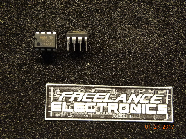
TS555IN
Part #
TS555IN
Description
Standard Timer Single 8-Pin PDIP Tube - Rail/Tube (Alt: TS
Category
IC
Availability
In Stock
Qty
22
Qty
Price
1 +
$0.54792
Manufacturer
Available
Qty
STMicroelectronics
Freelance Stock:
22
Ships Immediately
Add to Cart
Related Items
STMicroelectronics
IC
TS555IDT
$0.76230
Fairchild Semiconductor
IC
008-25424
$11.58351
Harris Corporation
IC
01-6945-9
Motorola Corp
IC
010-143121-0002
Texas Instruments
IC
01295-672141D
Military Spec
IC
01405915