Closed Dec 25th-26th
800-300-1968
We Stock Hard to Find Parts
My Account
|
My Orders
|
My Cart
Questions?
(800) 300-1968
Register
(current)
My Account
(current)
My Orders
(current)
My Cart
(current)
Categories
(current)
Manufacturers
Request a Quote
Sell Your Excess
Consignment
Quality Assurance
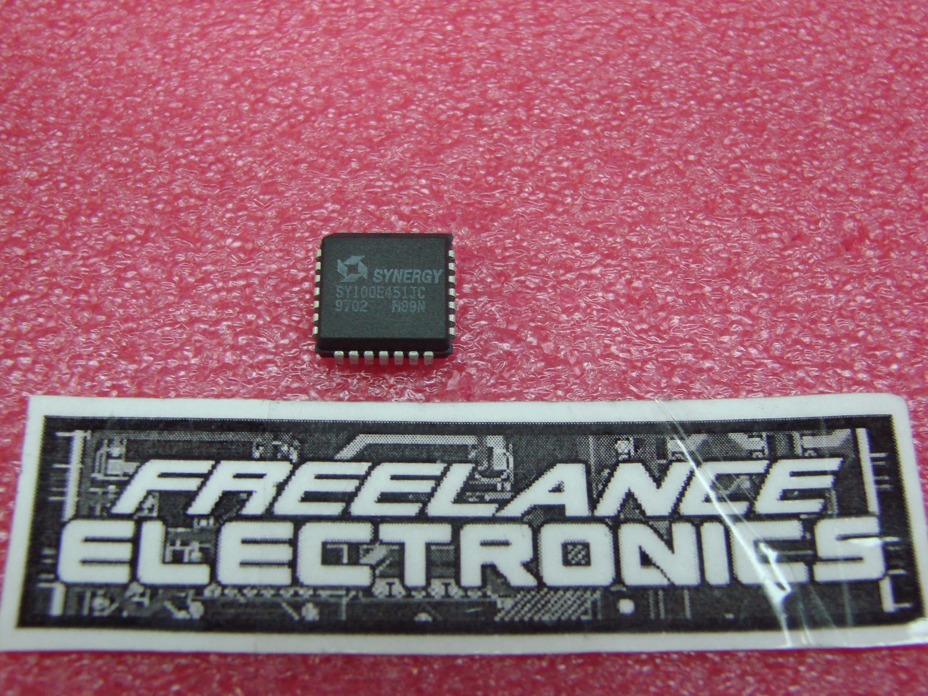
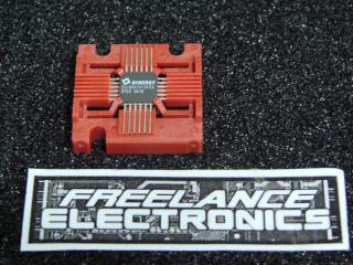
SY100E451JC
Part #
SY100E451JC
Description
IC D-TYPE POS TRG SNGL 28PLCC
Category
IC
Availability
In Stock
Qty
332
Qty
Price
1 - 15
$9.38273
16 - 39
$7.50618
40 - 88
$6.19260
89 - 134
$5.75474
135 +
$5.12922
Manufacturer
Available
Qty
SYNERGY
Date Code: 02
Freelance Stock:
323
Ships Immediately
SYNERGY
Date Code: 9132
Freelance Stock:
9
Ships Immediately
Add to Cart
Related Items
SYNERGY
IC
SY1001E131JC
SYNERGY
IC
SY100474-5FCS
SYNERGY
IC
SY100E016JC
$9.97117
SYNERGY
IC
SY100E111JC
$9.05120
SYNERGY
IC
SY100E137JC
$15.23256
SYNERGY
IC
SY100E150JC
$8.38484