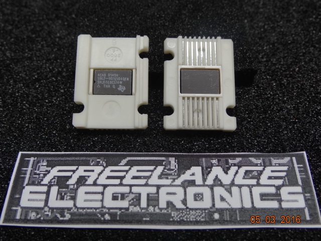
Freelance Electronics Components Distributor
Closed Dec 25th-26th
800-300-1968
We Stock Hard to Find Parts

SNJ55LBC174W

Part # SNJ55LBC174W
Description Quad Transmitter RS-485 16-Pin CFPAK Tube - Rail/Tube
Category IC
Availability In Stock
Qty 15
Qty Price
1 - 3 $47.40091
4 - 6 $37.70527
7 - 9 $35.55068
10 - 12 $33.03700
13 + $29.44602
Manufacturer Available Qty
Texas Instruments
Date Code: 0549
  • Shipping Freelance Stock: 15
    Ships Immediately


Technical Document


DISCLAIMER: The information provided herein is solely for informational purposes. Customers must be aware of the suitability of this product for their application, and consider that variable factors such as Manufacturer, Product Category, Date Codes, Pictures and Descriptions may differ from available inventory.


    
SGLS082A − MARCH 1995 − REVISED JULY 2004
1
POST OFFICE BOX 655303 DALLAS, TEXAS 75265
D Meets EIA Standard RS-485
D Designed for High-Speed Multipoint
Transmission on Long Bus Lines in Noisy
Environments
D Supports Data Rates up to and Exceeding
Ten Million Transfers Per Second
D Common-Mode Output Voltage Range of
7 V to 12 V
D Positive- and Negative-Current Limiting
D Low Power Consumption...1.5 mA Max
(Output Disabled)
description
The SN55LBC174 is composed of monolithic
quadruple differential line drivers with 3-state
outputs. This device is designed to meet the
requirements of the Electronics Industry
Association (EIA) Standard RS-485 and is
optimized for balanced multipoint bus
transmission at data rates up to and exceeding 10
million bits per second. Each driver features wide
positive and negative common-mode output
voltage ranges, current limiting, and
thermal-shutdown protection making it suitable
for party-line applications in noisy environments.
This device is designed using LinBiCMOS,
facilitating ultra-low power consumption and
inherent robustness.
The SN55LBC174 provides positive and negative-current limiting and thermal shutdown for protection from line
fault conditions on the transmission bus line. This device offers optimum performance when used with the
SN55LBC173 quadruple line receiver. The SN55LBC174 is available in the 16-pin CDIP package (J), the 16-pin
CPAK (W), or the 20-pin LCCC package (FK).
The SN55LBC174 is characterized for operation over the military temperature range of −55°C to 125°C.
FUNCTION TABLE
(each driver)
INPUT
ENABLE
OUTPUTS
INPUT
ENABLE
Y Z
H H H L
L H L H
X L Z Z
H = high level, L = low level, X = irrelevant,
Z = high impedance (off)
Copyright 2004, Texas Instruments Incorporated
   ! "#$ !  %#&'" ($)
(#"! "  !%$""! %$ *$ $!  $+! !#$!
!(( ,-) (#" %"$!!. ($!  $"$!!'- "'#($
$!.  '' %$$!)
1
2
3
4
5
6
7
8
16
15
14
13
12
11
10
9
1A
1Y
1Z
1,2EN
2Z
2Y
2A
GND
V
CC
4A
4Y
4Z
3,4EN
3Z
3Y
3A
J OR W PACKAGE
(TOP VIEW)
NC − No internal connection
FK PACKAGE
(TOP VIEW)
1920132
17
18
16
15
14
1312119 10
5
4
6
7
8
4Y
4Z
NC
3,4EN
3Z
1Z
1,2EN
NC
2Z
2Y
1Y
1A
NC
4A
GND
NC
3A
3Y
2A
V
CC
Please be aware that an important notice concerning availability, standard warranty, and use in critical applications of
Texas Instruments semiconductor products and disclaimers thereto appears at the end of this data sheet.
 %(#"! "%'  /0102 '' %$$! $ $!$(
#'$!! *$,!$ $()  '' *$ %(#"!2 %(#"
%"$!!. ($!  $"$!!'- "'#($ $!.  '' %$$!)
LinBiCMOS is a trademark of Texas Instruments Incorporated.

    
SGLS082A − MARCH 1995 − REVISED JULY 2004
2
POST OFFICE BOX 655303 DALLAS, TEXAS 75265
logic symbol
EN
EN
4A
3A
3,4EN
2A
1A
1,2EN
15
9
12
7
1
4
4Z
4Y
3Z
3Y
2Z
2Y
1Z
1Y
13
14
11
10
5
6
3
2
This symbol is in accordance with ANSI/IEEE Std 91-1984
and IEC publication 617-12.
Pin numbers shown are for the J or W package.
logic diagram (positive logic)
1A
1Y
1Z
2A
2Y
2Z
1,2EN
3A
3Y
3Z
4A
4Y
4Z
3,4EN
1
4
7
9
12
15
13
14
11
10
5
6
3
2
schematic of inputs and outputs
Input
50 µA
V
CC
Driver
Output
V
CC
200
ALL INPUTS Y OR Z OUTPUT

    
SGLS082A − MARCH 1995 − REVISED JULY 2004
3
POST OFFICE BOX 655303 DALLAS, TEXAS 75265
absolute maximum ratings over operating free-air temperature (unless otherwise noted)
Supply voltage range, V
CC
(see Note 1) 0.3 V to 7 V. . . . . . . . . . . . . . . . . . . . . . . . . . . . . . . . . . . . . . . . . . . . . .
Output voltage range, V
O
10 V to 15 V. . . . . . . . . . . . . . . . . . . . . . . . . . . . . . . . . . . . . . . . . . . . . . . . . . . . . . . . . . .
Input voltage range, V
I
0.3 V to 7 V. . . . . . . . . . . . . . . . . . . . . . . . . . . . . . . . . . . . . . . . . . . . . . . . . . . . . . . . . . . . . .
Continuous power dissipation Internally limited
. . . . . . . . . . . . . . . . . . . . . . . . . . . . . . . . . . . . . . . . . . . . . . . . . . . .
Operating free-air temperature range, T
A
−55°C to 125°C. . . . . . . . . . . . . . . . . . . . . . . . . . . . . . . . . . . . . . . . . . .
Storage temperature range, T
stg
−65°C to 150°C. . . . . . . . . . . . . . . . . . . . . . . . . . . . . . . . . . . . . . . . . . . . . . . . . . .
Lead temperature 1,6 mm (1/16 inch) from case for 10 seconds 65°C to 150°C. . . . . . . . . . . . . . . . . . . . . . .
Stresses beyond those listed under “absolute maximum ratings” may cause permanent damage to the device. These are stress ratings only, and
functional operation of the device at these or any other conditions beyond those indicated under “recommended operating conditions” is not
implied. Exposure to absolute-maximum-rated conditions for extended periods may affect device reliability.
The maximum operating junction temperature is internally limited. Use the dissipation rating table to operate below this temperature.
NOTE 1: All voltage values are with respect to GND.
DISSIPATION RATING TABLE
PACKAGE
T
A
25°C
POWER RATING
DERATING FACTOR
ABOVE T
A
= 25°C
T
A
= 125°C
POWER RATING
FK 1375 mW 11 mW/°C 275 mW
J 1375 mW 11 mW/°C 275 mW
W 1000 mW 8 mW/°C 200 mW
recommended operating conditions
MIN NOM MAX UNIT
Supply voltage, V
CC
4.75 5 5.25 V
High-level input voltage, V
IH
2 V
Low-level input voltage, V
IL
0.8 V
Voltage at any bus terminal (separately or common mode), V
O
Y or Z
12
V
Voltage at any bus terminal (separately or common mode), V
O
Y or Z
−7
V
High-level output current, I
OH
Y or Z −60 mA
Low-level output current, I
OL
Y or Z 60 mA
Operating free-air temperature, T
A
−55 125 °C
12345NEXT