Freelance Electronics Components Distributor
Closed Dec 25th-26th
800-300-1968
We Stock Hard to Find Parts

OPA349UA

Part # OPA349UA
Description OP Amp Single GP R-R I/O 5.5V8-Pin SOIC Tube (Alt: OPA349
Category IC
Availability In Stock
Qty 86
Qty Price
1 - 18 $0.75203
19 - 36 $0.59821
37 - 54 $0.56402
55 - 72 $0.52414
73 + $0.46717
Manufacturer Available Qty
Texas Instruments
Date Code: 0714
  • Shipping Freelance Stock: 86
    Ships Immediately


Technical Document


DISCLAIMER: The information provided herein is solely for informational purposes. Customers must be aware of the suitability of this product for their application, and consider that variable factors such as Manufacturer, Product Category, Date Codes, Pictures and Descriptions may differ from available inventory.

1µA, Rail-to-Rail I/O CMOS
OPERATIONAL AMPLIFIERS
FEATURES
LOW SUPPLY CURRENT: 1µA
GAIN-BANDWIDTH: 70kHz
UNITY-GAIN STABLE
LOW INPUT BIAS CURRENT: 10pA (max)
WIDE SUPPLY RANGE: 1.8V to 5.5V
INPUT RANGE: 200mV Beyond Rails
OUTPUT SWINGS TO 350mV OF RAILS
OUTPUT DRIVE CURRENT: 8mA
OPEN-LOOP GAIN: 90dB
Micro
PACKAGES: SC70, SOT23-5, SOT23-8
APPLICATIONS
BATTERY PACKS AND POWER SUPPLIES
PORTABLE PHONES, PAGERS, AND CAMERAS
SOLAR-POWERED SYSTEMS
SMOKE, GAS, AND FIRE DETECTION SYSTEMS
REMOTE SENSORS
PCMCIA CARDS
DRIVING ANALOG-TO-DIGITAL (A/D) CONVERTERS
Micro
POWER FILTERS
DESCRIPTION
The OPA349 and OPA2349 are ultra-low power operational
amplifiers that provide 70kHz bandwidth with only 1µA quies-
cent current. These rail-to-rail input and output amplifiers are
specifically designed for battery-powered applications. The
input common-mode voltage range extends 200mV beyond
the power-supply rails and the output swings to within 350mV
of the rails, maintaining wide dynamic range. Unlike some
micropower op amps, these parts are unity-gain stable and
require no external compensation to achieve wide band-
width. The OPA349 features a low input bias current that
allows the use of large source and feedback resistors.
The OPA349 can be operated with power supplies from 1.8V
to 5.5V with little change in performance, ensuring continuing
superior performance even in low battery situations.
The OPA349 comes in miniature SOT23-5, SC70, and SO-8
surface-mount packages. The OPA2349 dual is available in
SOT23-8, and SO-8 surface-mount packages. These tiny
packages are ideal for use in high-density applications, such
as PCMCIA cards, battery packs, and portable instruments.
The OPA349 is specified for 0°C to +70°C. The OPA2349 is
specified for –40°C to +70°C.
OPA349
OPA2349
SBOS121B – JUNE 2000 – REVISED JANUARY 2004
PRODUCTION DATA information is current as of publication date.
Products conform to specifications per the terms of Texas Instruments
standard warranty. Production processing does not necessarily include
testing of all parameters.
Copyright © 2000-2004, Texas Instruments Incorporated
FEATURES PRODUCT
1µA, 5.5kHz, Rail-To-Rail TLV240x
1µA, 5.5kHz, Rail-To-Rail TLV224x
7µA, 160kHz, Rail-To-Rail, 2.7V to 16V Supply TLV238x
7µA, 160kHz, Rail-To-Rail, Micro Power TLV27Lx
20µA, 500kHz, Rail-To-Rail, 1.8V Micro Power TLV276x
20µA, 350kHz, Rail-To-Rail, Micro Power OPAx347
45µA, 1MHz, Rail-To-Rail, 2.1V to 5.5V Supply OPAx348
OPAx349 RELATED PRODUCTS
OPA349
O
P
A
2
34
9
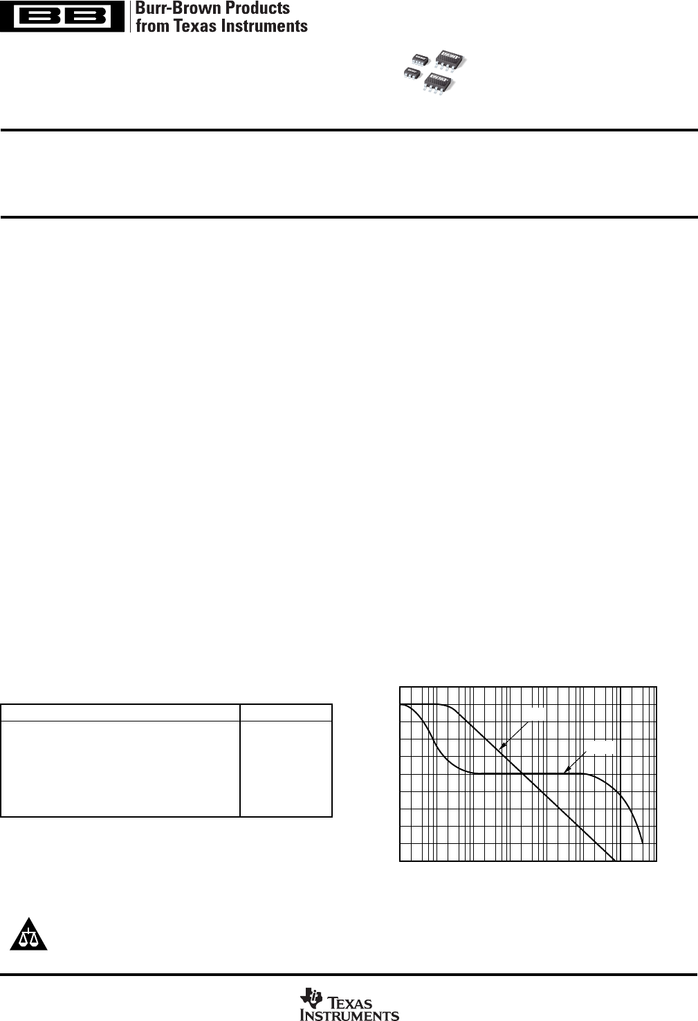
OPEN-LOOP GAIN AND PHASE vs FREQUENCY
Frequency (Hz)
Gain (dB)
Phase (°)
100
90
80
70
60
50
40
30
20
10
0
0
45
90
135
180
1 10 100 1k 10k 100k 1M0.1
Gain
Phase
www.ti.com
Please be aware that an important notice concerning availability, standard warranty, and use in critical applications of
Texas Instruments semiconductor products and disclaimers thereto appears at the end of this data sheet.
All trademarks are the property of their respective owners.
OPA349, 2349
2
SBOS121B
www.ti.com
Supply Voltage, V+ to V ................................................................... 5.5V
Signal Input Terminals, Voltage
(2)
.................. (V) 0.5V to (V+) + 0.5V
Current
(2)
.................................................... 10mA
Output Short Circuit
(3)
.............................................................. Continuous
Operating Temperature, OPA2349 ................................55°C to +125°C
Operating Temperature, OPA349 ........................................0°C to +85°C
Storage Temperature .....................................................65°C to +150°C
Junction Temperature ...................................................................... 150°C
Lead Temperature (soldering, 3s) ................................................... 300°C
NOTES: (1) Stresses above these ratings may cause permanent damage.
Exposure to absolute maximum conditions for extended periods may de-
grade device reliability. These are stress ratings only, and functional opera-
tion of the device at these, or any other conditions beyond those specified,
is not implied. (2) Input terminals are diode-clamped to the power-supply
rails. Input signals that can swing more than 0.5V beyond the supply rails
should be current-limited to 10mA or less. (3) Short-circuit to ground, one
amplifier per package.
ABSOLUTE MAXIMUM RATINGS
(1)
PACKAGE/ORDERING INFORMATION
(1)
PACKAGE PACKAGE ORDERING TRANSPORT
PRODUCT PACKAGE DESIGNATOR
(1)
MARKING NUMBER MEDIA, QUANTITY
Single
OPA349NA SOT23-5 DBV A49 OPA349NA/250 Tape and Reel, 250
""" "OPA349NA/3K Tape and Reel, 3000
OPA349UA SO-8 D OPA349UA OPA349UA Rails, 100
""" "OPA349UA/2K5 Tape and Reel, 2500
OPA349SA SC70-5 DCK S49 OPA349SA/250 Tape and Reel, 250
""" "OPA349SA/3K Tape and Reel, 3000
Dual
OPA2349EA SOT23-8 DCN C49 OPA2349EA/250 Tape and Reel, 250
""" "OPA2349EA/3K Tape and Reel, 3000
OPA2349UA SO-8 D OPA2349UA OPA2349UA Rails, 100
""" "OPA2349UA/2K5 Tape and Reel, 2500
NOTE: (1) For the most current package and ordering information, see the Package Option Addendum located at the end of this data sheet.
1
2
3
5
4
V+
In
Out
V
+In
OPA349
SOT23-5
1
2
3
4
8
7
6
5
NC
(1)
V+
Out
NC
(1)
NC
(1)
In
+In
V
OPA349
SO-8
1
2
3
4
8
7
6
5
V+
Out B
In B
+In B
Out A
In A
+In A
V
OPA2349
SOT23-8, SO-8
ELECTROSTATIC
DISCHARGE SENSITIVITY
This integrated circuit can be damaged by ESD. Texas Instru-
ments recommends that all integrated circuits be handled with
appropriate precautions. Failure to observe proper handling
and installation procedures can cause damage.
ESD damage can range from subtle performance degrada-
tion to complete device failure. Precision integrated circuits
may be more susceptible to damage because very small
parametric changes could cause the device not to meet its
published specifications.
PIN CONFIGURATIONS
NOTE: (1) NC indicates no internal connection.
1
2
3
5
4
V+
Out
+In
V
In
OPA349
SC70-5
OPA349, 2349
3
SBOS121B
www.ti.com
ELECTRICAL CHARACTERISTICS (Single): V
S
= +1.8V to +5.5V
Boldface limits apply over the specified temperature range, T
A
= 0°C to +70°C.
At T
A
= +25°C, and R
L
= 1M connected to V
S
/2, unless otherwise noted.
PARAMETER CONDITION MIN TYP
(1)
MAX UNITS
OFFSET VOLTAGE
Input Offset Voltage V
OS
V
S
= 5V, V
CM
= 2.5V ±2 ±10 mV
Over Temperature
±2 ±13 mV
Drift dV
OS
/dT ±15 µV/°C
vs Power-Supply Rejection Ratio PSRR V
S
= 1.8V to 5.5V, V
CM
= (V) + 0.3V 350 1000 µV/V
Over Temperature 3000
µV/V
INPUT VOLTAGE RANGE
Common-Mode Voltage Range V
CM
(V) 0.2 (V+) + 0.2 V
Common-Mode Rejection Ratio CMRR V
S
= +5V, 0.2V < V
CM
< 5.2V 48 60 dB
Over Temperature 46 dB
V
S
= +5V, 0.2V < V
CM
< 3.5V 52 72 dB
Over Temperature 50 dB
INPUT BIAS CURRENT
Input Bias Current I
B
±0.5 ±10 pA
Input Offset Current I
OS
±1 ±10 pA
INPUT IMPEDANCE
Differential 10
13
|| 2 || pF
Common-Mode 10
13
|| 4 || pF
NOISE
Input Voltage Noise, f = 0.1Hz to 10Hz 8 µVp-p
Input Voltage Noise Density, f = 1kHz e
n
300 nV/Hz
Current Noise Density, f = 1kHz i
n
4fA/Hz
OPEN-LOOP GAIN
Open-Loop Voltage Gain A
OL
R
L
= 1M, V
S
= +5.5V, +0.3V < V
O
< +5.2V
74 90 dB
Over Temperature 72 dB
Open-Loop Voltage Gain A
OL
R
L
= 10k, V
S
= +5.5V, +0.35V < V
O
< +5.15V
74 90 dB
Over Temperature 60 dB
OUTPUT
Voltage Output Swing from Rail R
L
= 1M, V
S
= +5.5V, A
OL
> 74dB 300 mV
Over Temperature 300 mV
R
L
= 10k, V
S
= +5.5V, A
OL
> 74dB 350 mV
Over Temperature 350 mV
Output Current ±8mA
Short-Circuit Current I
SC
±10 mA
Capacitive Load Drive C
LOAD
See Typical Characteristics
FREQUENCY RESPONSE C
L
= 10pF
Gain-Bandwidth Product GBW G = +1 70 kHz
Slew Rate SR V
S
= +5V, G = +1 0.02 V/µs
Settling Time, 0.1% t
S
V
S
= 5V, 1V Step 65 µs
0.01% V
S
= 5V, 1V Step 80 µs
Overload Recovery Time V
IN
Gain = V
S
5 µs
POWER SUPPLY
Specified Voltage Range V
S
+1.8 +5.5 V
Quiescent Current (per amplifier) I
Q
I
O
= 0 1 2 µA
Over Temperature 10
µA
TEMPERATURE RANGE
Specified Range 0 +70 °C
Operating Range 0 +85 °C
Storage Range 65 +150 °C
Thermal Resistance
θ
JA
SOT23-5 Surface-Mount 200 °C/W
SO-8 Surface-Mount 150 °C/W
SC70-5 Surface-Mount 250 °C/W
OPA349
NOTE: (1) Refer to Typical Characteristic curves.
1234567NEXT