Product Specification
PE97022
Page 10 of 14
©2007-2008 Peregrine Semiconductor Corp. All rights reserved.
Document No. 70-0235-04 │ UltraCMOS™ RFIC Solutions
Serial Interface Mode
Serial Interface Mode is selected by setting the
Bmode input “low” and the Smode input “high”.
While the E_WR input is “low” and the S_WR
input is “low”, serial input data (Sdata input), B
0
to
B
19
, is clocked serially into the primary register on
the rising edge of Sclk, MSB (B
0
) first. The
contents from the primary register are transferred
into the secondary register on the rising edge of
either S_WR or Hop_WR according to the timing
diagram shown in Figure 7. Data is transferred to
the counters as shown in Table 7.
The double buffering provided by the primary and
secondary registers allows for “ping-pong” counter
control using the FSELS input. When FSELS is
“high”, the primary register contents set the
counter inputs. When FSELS is “low”, the
secondary register contents are utilized.
While the E_WR input is “high” and the S_WR
input is “low”, serial input data (Sdata input), B
0
to
B
7
, is clocked serially into the enhancement
register on the rising edge of Sclk, MSB (B
0
) first.
The enhancement register is double buffered to
prevent inadvertent control changes during serial
loading, with buffer capture of the serially-entered
data performed on the falling edge of E_WR
according to the timing diagram shown in
Figure 6. After the falling edge of E_WR, the data
provides control bits as shown in Table 8 with bit
functionality enabled by asserting the Enh input
“low”.
Direct Interface Mode
Direct Interface Mode is selected by setting the
Bmode input “high”.
Counter control bits are set directly at the pins as
shown in Table 7. In Direct Interface Mode, main
counter inputs M
7
and M
8
, and R Counter inputs
R
4
and R
5
are internally forced low (“0”).
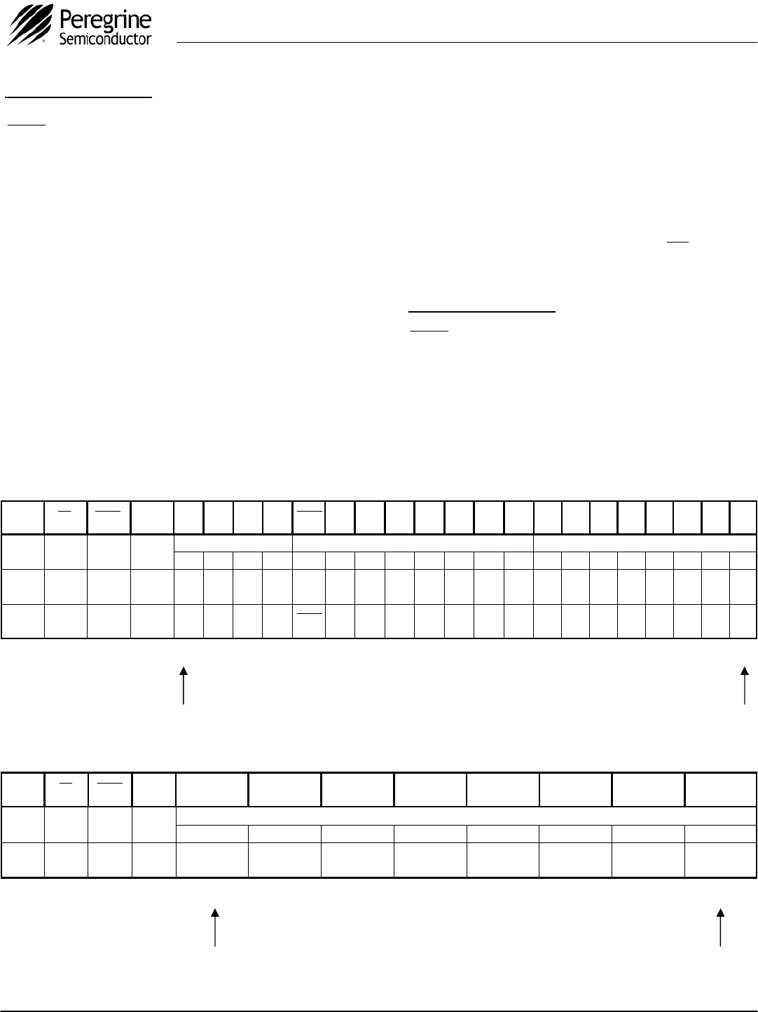
MSB (first in) (last in) LSB
Table 7. Primary Register Programming
Table 8. Enhancement Register Programming
*Serial data clocked serially on Sclk rising edge while E_WR “low” and captured in secondary register on S_WR rising edge.
*Serial data clocked serially on Sclk rising edge while E_WR “high” and captured in the double buffer on E_WR falling edge.
MSB (first in) (last in) LSB
Interface
Mode
Enh Bmode
Smode R
5
R
4
M
8
M
7
Pre_en
M
6
M
5
M
4
M
3
M
2
M
1
M
0
R
3
R
2
R
1
R
0
A
3
A
2
A
1
A
0
Parallel 1 0 0
M2_WR rising edge load M1_WR rising edge load A_WR rising edge load
D
3
D
2
D
1
D
0
D
7
D
6
D
5
D
4
D
3
D
2
D
1
D
0
D
7
D
6
D
5
D
4
D
3
D
2
D
1
D
0
Serial* 1 0 1 B
0
B
1
B
2
B
3
B
4
B
5
B
6
B
7
B
8
B
9
B
10
B
11
B
12
B
13
B
14
B
15
B
16
B
17
B
18
B
19
Direct 1 1 X 0 0 0 0 Pre_en M
6
M
5
M
4
M
3
M
2
M
1
M
0
R
3
R
2
R
1
R
0
A
3
A
2
A
1
A
0
Interface
Mode
Enh Bmode
Smode Reserved Reserved Reserved
Power
down
Counter
load
MSEL
output
Prescaler
output
f
c
, f
p
OE
Parallel 0 0 0
E_WR rising edge load
D
7
D
6
D
5
D
4
D
3
D
2
D
1
D
0
Serial* 0 0 1 B
0
B
1
B
2
B
3
B
4
B
5
B
6
B
7


