Product Specification
PE97022
Page 6 of 14
©2007-2008 Peregrine Semiconductor Corp. All rights reserved.
Document No. 70-0235-04 │ UltraCMOS™ RFIC Solutions
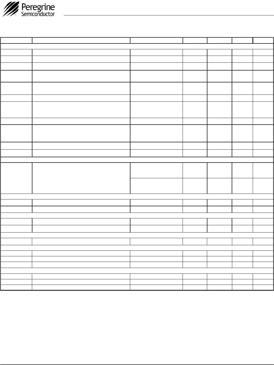
Table 6. AC Characteristics: V
DD
= 3.3 V, -40° C < T
A
< 85° C, unless otherwise specified
Note 1: Fclk is verified during the functional pattern test. Serial programming sections of the functional pattern are clocked at 10 MHz to verify Fclk
specification.
Note 2: CMOS logic levels can be used to drive reference input if DC coupled. Voltage input needs to be a minimum of 0.5Vp-p.
Note 3: Parameter is guaranteed through characterization only and is not tested.
Note 4: Parameters below are not tested for die sales. These parameters are verified during the element evaluation.
Symbol Parameter Conditions Min Typical Max Units
Control Interface and Latches (see Figures 4, 5, 6)
f
Clk
Serial data clock frequency (Note 1) 10 MHz
t
ClkH
Serial clock HIGH time 30 ns
t
ClkL
Serial clock LOW time 30 ns
t
DSU
Sdata set-up time after Sclk rising edge, D[7:0] set-up
time to M1_WR, M2_WR, A_WR, E_WR rising edge
10 ns
t
DHLD
Sdata hold time after Sclk rising edge, D[7:0] hold
time to M1_WR, M2_WR, A_WR, E_WR rising edge
10 ns
t
PW
S_WR, M1_WR, M2_WR, A_WR, E_WR pulse width 30 ns
t
CWR
Sclk rising edge to S_WR rising edge. S_WR,
M1_WR, M2_WR, A_WR falling edge to Hop_WR
rising edge
30 ns
t
CE
Sclk falling edge to E_WR transition 30 ns
t
WRC
S_WR falling edge to Sclk rising edge. Hop_WR
falling edge to S_WR, M1_WR, M2_WR, A_WR rising
edge
30 ns
t
EC
E_WR transition to Sclk rising edge 30 ns
t
MDO
MSEL data out delay after Fin rising edge C
L
= 12 pf 8 ns
Main Divider (Including Prescaler) (Note 4)
P
Fin
Input level range
External AC coupling
275 MHz ≤ Freq ≤ 3200MHz
-5 5 dBm
External AC coupling
3.2 GHz < Freq ≤ 3.5 GHz
3.15 V ≤ VDD ≤ 3.45 V
0 5 dBm
Main Divider (Prescaler Bypassed) (Note 4)
F
in
Operating frequency 50 300 MHz
P
Fin
Input level range External AC coupling -5 5 dBm
Reference Divider
f
r
Operating frequency (Note 3) 100 MHz
P
fr
Reference input power (Note 2) Single-ended input -2 10 dBm
Phase Detector
f
c
Comparison frequency (Note 3) 50 MHz
SSB Phase Noise (F
in
= 1.9 GHz, f
r
= 20 MHz, f
c
= 20 MHz, LBW = 50 kHz, V
DD
= 3.3 V, Temp = 25° C) (Note 4)
Φ
N
Phase Noise 100 Hz Offset -89 dBc/Hz
Φ
N
Phase Noise 1 kHz Offset -95 dBc/Hz
Φ
N
Phase Noise 10 kHz Offset -102 dBc/Hz
SSB Phase Noise (F
in
= 1.9 GHz, f
r
= 20 MHz, f
c
= 20 MHz, LBW = 50 kHz, V
DD
= 3.0 V, Temp = 25° C) (Note 4)
Φ
N
Phase Noise 100 Hz Offset -87 dBc/Hz
Φ
N
Phase Noise 1 kHz Offset -94 dBc/Hz
Φ
N
Phase Noise 10 kHz Offset -101 dBc/Hz


