Closed Dec 25th-26th
800-300-1968
We Stock Hard to Find Parts
My Account
|
My Orders
|
My Cart
Questions?
(800) 300-1968
Register
(current)
My Account
(current)
My Orders
(current)
My Cart
(current)
Categories
(current)
Manufacturers
Request a Quote
Sell Your Excess
Consignment
Quality Assurance
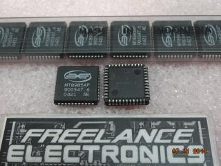
MT8985AE
Part #
MT8985AE
Description
Switch Fabric 256 x 256 16.384Mbps 5V 40-Pin PDIP Tube
Category
IC
Availability
In Stock
Qty
3
Qty
Price
1 +
$7.17208
Manufacturer
Available
Qty
MITEL
Date Code: 9605
Freelance Stock:
3
Ships Immediately
Add to Cart
Related Items
ZARLINK
IC
MT8980DC
ZARLINK
IC
MT8980DE
$6.99138
ZAR
IC
MT8985AP
$12.85771
Fairchild Semiconductor
IC
008-25424
$11.58351
Harris Corporation
IC
01-6945-9
Motorola Corp
IC
010-143121-0002