Closed Dec 25th-26th
800-300-1968
We Stock Hard to Find Parts
My Account
|
My Orders
|
My Cart
Questions?
(800) 300-1968
Register
(current)
My Account
(current)
My Orders
(current)
My Cart
(current)
Categories
(current)
Manufacturers
Request a Quote
Sell Your Excess
Consignment
Quality Assurance
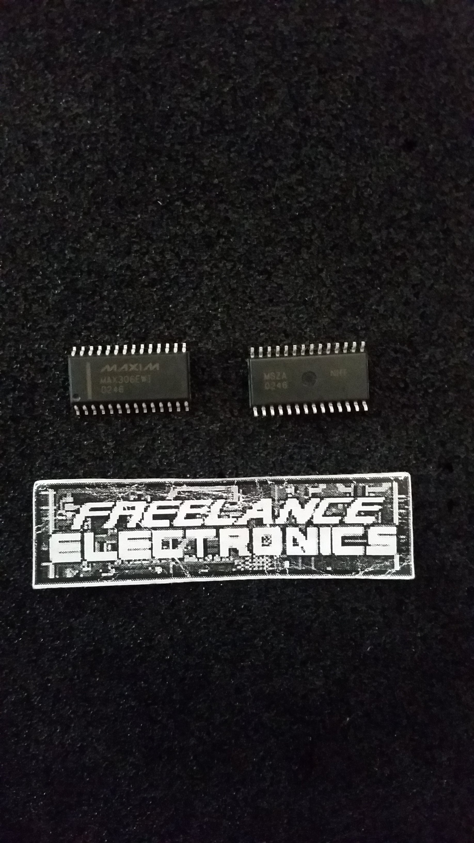
MAX306EWI
Part #
MAX306EWI
Description
Multiplexer Switch ICs Precision, 16-Channel/Dual
Category
IC
Availability
Out of Stock
Qty
0
Qty
Price
1 +
$4.77759
Related Items
MAXIM
IC
MAX3023EUD+
$6.35187
MAXIM
IC
MAX3030EEUE
$4.14661
MAXIM
IC
MAX3033EESE
$1.49472
MAXIM
IC
MAX303ESE
$13.08515
MAXIM
IC
MAX303MJE
$8.03608
MAXIM
IC
MAX3043EUE
$13.26003