Closed Dec 25th-26th
800-300-1968
We Stock Hard to Find Parts
My Account
|
My Orders
|
My Cart
Questions?
(800) 300-1968
Register
(current)
My Account
(current)
My Orders
(current)
My Cart
(current)
Categories
(current)
Manufacturers
Request a Quote
Sell Your Excess
Consignment
Quality Assurance
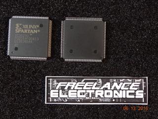
XC3S200-4FTG256I
Part #
XC3S200-4FTG256I
Description
FPGA SPARTAN-3 200K GATES 4320 CELLS 630MHZ 1.2V 256FTBGA
Category
IC
Availability
Out of Stock
Qty
0
Qty
Price
1 +
$27.30617
Related Items
Xilinx
IC
XC3S200-4FT256C
$17.84582
Xilinx
IC
XC3S200-4PQ208C
$20.88685
Xilinx
IC
XC3S200-4TQG144C
$17.90506
Xilinx
IC
XC3S200-4VQ100C
$27.85030
Xilinx
IC
XC3S2000-4FG676I
$106.32876
Xilinx
IC
XC3S200AN-4FTG256C
$17.87256