Freelance Electronics Components Distributor
Closed Dec 25th-26th
800-300-1968
We Stock Hard to Find Parts

VCA810ID

Part # VCA810ID
Description SINGLE VOLTAGE CONTROL AMP -Rail/Tube
Category IC
Availability Out of Stock
Qty 0


Technical Document


DISCLAIMER: The information provided herein is solely for informational purposes. Customers must be aware of the suitability of this product for their application, and consider that variable factors such as Manufacturer, Product Category, Date Codes, Pictures and Descriptions may differ from available inventory.

VCA810
SBOS275F JUNE 2003REVISED DECEMBER 2010
www.ti.com
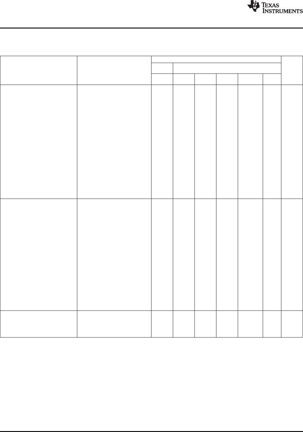
ELECTRICAL CHARACTERISTICS: V
S
= ±5V (continued)
Boldface limits are tested at +25°C.
At R
L
= 500, and V
IN
= single-ended input on V+ with V at ground,, unless otherwise noted.
VCA810
MIN/MAX OVER
TYP TEMPERATURE
0°C to –40°C to MIN/ TEST
PARAMETER CONDITIONS +25°C +25°C
(2)
+70°C
(3)
+85°C
(3)
UNITS MAX LEVEL
(1)
GAIN CONTROL (V
C
, Pin 3) Single-ended or differential input
Specified gain range ΔV
C
/ΔdB = 25mV/dB ±40 dB typ C
Maximum control voltage G = 40dB 0 V typ C
Minimum control voltage G = +40dB –2 V typ C
Gain accuracy 1.8V V
C
0.2V ±0.4 ±1.5 ±2.5 ±3.5 dB max A
V
C
< 1.8V, V
C
> 0.2V ±0.5 ±2.2 ±3.7 ±4.7 dB max A
Gain drift 1.8V V
C
0.2V ±0.02 ±0.03 dB/°C max B
V
C
< 1.8V, V
C
> 0.2V ±0.03 ±0.04 dB/°C max B
Gain control slope 40 db/V typ C
Gain control linearity
(6)
1.8V V
C
0V ±0.3 ±1 ±1.1 ±1.2 dB max A
V
C
< 1.8V ±0.7 ±1.6 ±2.5 ±3.2 dB max A
Gain control bandwidth 25 20 19 19 MHz min B
Gain control slew rate 80dB Gain Step 900 dB/ns typ C
Gain settling time 1%, 80dB Step 0.8 ms typ C
Input bias current V
C
= 1V –1.5 –3.5 –4.5 –8 mA max A
Gain + Power-supply rejection ratio V
C
= 2V, G = +40dB, +V
S
= 5V ±0.5V 0.5 1.5 1.8 2 dB/V max A
Gain – Power-supply rejection ratio V
C
= 2V, G = +40dB, –V
S
= –5V ±0.5V 0.7 1.5 1.8 2 dB/V max A
POWER SUPPLY
Specified operating voltage ±5 V typ C
Minimum operating voltage ±4 ±4 ±4 V min A
Maximum operating voltage ±6 ±6 ±6 V max A
Positive supply quiescent current
Maximum quiescent current +V
S
= +5V, G = 40dB 10 12.5 12.6 12.7 mA min A
Minimum quiescent current +V
S
= +5V, G = 40dB 10 7.5 7.2 7.1 mA max A
Maximum quiescent current +V
S
= +5V, G = +40dB 18 20.5 22 22.3 mA min A
Minimum quiescent current +V
S
= +5V, G = +40dB 18 15.5 14.5 13.5 mA max A
Negative supply quiescent current
(7)
Maximum quiescent current V
S
= 5V, G = 40dB 12 14.5 14.6 14.7 mA max A
Minimum quiescent current V
S
= 5V, G = 40dB 12 9.5 9.4 9.3 mA min A
Maximum quiescent current V
S
= 5V, G = +40dB 20 22.5 24.5 24.8 mA max A
Minimum quiescent current V
S
= 5V, G = +40dB 20 17.5 16.5 16 mA min A
Positive power-supply rejection ratio (+PSRR) Input-referred, V
C
= 2V 90 75 75 73 dB min A
Negative power-supply rejection ratio
Input-referred, V
C
= 2V 85 70 70 68 dB min A
(–PSRR)
THERMAL CHARACTERISTICS
Specified operating range, ID package –40 to +85 °C typ C
Thermal resistance, q
JA
Junction-to-ambient
D SO-8 80 °C/W typ C
(6) Maximum deviation from best line fit.
(7) Magnitude.
4 Submit Documentation Feedback Copyright © 2003–2010, Texas Instruments Incorporated
Product Folder Link(s): VCA810
VCA810
www.ti.com
SBOS275F JUNE 2003REVISED DECEMBER 2010
HIGH GRADE DC SPECIFICATIONS: V
S
= ±5V (VCA810AID)
Boldface limits are tested at +25°C.
At R
L
= 500, and V
IN
= single-ended input on V+ with V at ground,, unless otherwise noted.
VCA810AID
MIN/MAX OVER
TYP TEMPERATURE
0°C to –40°C to MIN/ TEST
PARAMETER CONDITIONS +25°C +25°C
(2)
+70°C
(3)
+85°C
(3)
UNITS MAX LEVEL
(1)
DC PERFORMANCE Single-ended or differential input
Output offset voltage 2V < V
C
< 0V ±4 ±14 ±24 ±26 mV max A
Input offset voltage ±0.1 ±0.2 ±0.25 ±0.3 mV max A
Input offset current ±100 ±500 ±600 ±700 mA max A
GAIN CONTROL (V
C
, Pin 3) Single-ended or differential input
Gain accuracy 1.8V V
C
0.2V ±0.4 ±0.9 ±1.9 ±2.9 dB max A
V
C
< 1.8V, V
C
> 0.2V ±0.5 ±1.5 ±3.0 ±4.0 dB max A
Gain control linearity
(4)
1.8V V
C
0V ±0.3 ±0.6 ±0.7 ±0.8 dB max A
V
C
< 1.8V ±0.7 ±1.1 ±1.9 ±2.7 dB/V max A
POWER SUPPLY
Positive supply quiescent current
Maximum quiescent current +V
S
= +5V, G = 40dB 10 11.5 11.6 11.7 mA min A
Minimum quiescent current +V
S
= +5V, G = 40dB 10 8.5 8.2 8.1 mA max A
Maximum quiescent current +V
S
= +5V, G = +40dB 18 19.5 21 21.3 mA min A
Minimum quiescent current +V
S
= +5V, G = +40dB 18 16.5 15.5 14.5 mA max A
Negative supply quiescent current
(5)
Maximum quiescent current V
S
= 5V, G = 40dB 12 14 14.1 14.2 mA min A
Minimum quiescent current V
S
= 5V, G = 40dB 12 10 9.9 9.8 mA max A
Maximum quiescent current V
S
= 5V, G = +40dB 20 22 24 24.3 mA min A
Minimum quiescent current V
S
= 5V, G = +40dB 20 18 17 16.5 mA max A
(1) Test levels: (A) 100% tested at +25°C. Over temperature limits set by characterization and simulation. (B) Limits set by characterization
and simulation. (C) Typical value; only for information.
(2) Junction temperature = ambient for +25°C tested specifications.
(3) Junction temperature = ambient at low temperature limit; junction temperature = ambient +30°C at high temperature limit for over
temperature specifications.
(4) Maximum deviation from best line fit.
(5) Magnitude.
Copyright © 2003–2010, Texas Instruments Incorporated Submit Documentation Feedback 5
Product Folder Link(s): VCA810
60
40
20
0
20
40
60
-
-
-
Gain (dB)
Frequency (MHz)
1 10 100 1000
V = 10mV , V = 1V
IN PP OUT PP
V = 100m ,V VV = 1
IN PP OUT PP
V = 1 ,V VV = 1
IN PP OUT PP
V = 2 , VV V= 200m
OUT PP IN PP
V = 2 , VV V= 20m
OUT PP IN PP
Frequency (MHz)
1 10 100
R = 500W
L
V = 1V- + 10mV
C DC PP
3
0
3
6
9
12
15
18-
-
-
-
-
-
Gain (dB)
Time (20ns/div)
V = 2V
IN PP
G = 20dB-
G = 40dB-
Output Voltage (mV)
150
100
50
0
50
100
150-
-
-
Time (20ns/div)
V = 10mV
IN PP
G = +40dB
G = +20dB
Output Voltage (V)
0.6
0.4
0.2
0
0.2
0.4
0.6
-
-
-
1.2
1.0
0.8
0.6
0.4
0.2
0
0.2-
Output Voltage (V)
Time (20ns/div)
G = 0dB to 40dB, V = 1V-
IN DC
G = 0dB to +40dB, V = 10mV
IN DC
60
40
20
0
20
40
60
80
100
-
-
-
-
-
Gain (dB)
Control Voltage, V (V)
C
0.5 0 -0.5 -1.0 -2.0-1.5 -2.5
Specified Operating Range
Output Disabled for
+0.15V V£ £ +2V
C
VCA810
SBOS275F JUNE 2003REVISED DECEMBER 2010
www.ti.com
TYPICAL CHARACTERISTICS: V
S
= ±5V
At R
L
= 500 and V
IN
= single-ended input on V+ with V at ground, unless otherwise noted.
SMALLSIGNAL FREQUENCY RESPONSE GAIN CONTROL FREQUENCY RESPONSE
Figure 1. Figure 2.
ATTENUATED PULSE RESPONSE HIGH GAIN PULSE RESPONSE
Figure 3. Figure 4.
GAIN CONTROL PULSE RESPONSE GAIN vs CONTROL VOLTAGE
Figure 5. Figure 6.
6 Submit Documentation Feedback Copyright © 2003–2010, Texas Instruments Incorporated
Product Folder Link(s): VCA810
PREVIOUS12345678NEXT