Freelance Electronics Components Distributor
Closed Dec 25th-26th
800-300-1968
We Stock Hard to Find Parts

UCC2946D

Part # UCC2946D
Description MICRO SUPER W/ WATCHDOG TIMER- Rail/Tube
Category IC
Availability In Stock
Qty 385
Qty Price
1 - 80 $2.76393
81 - 161 $2.19858
162 - 242 $2.07295
243 - 323 $1.92638
324 + $1.71699
Manufacturer Available Qty
UNITRODE
  • Shipping Freelance Stock: 370
    Ships Immediately
UNITRODE
  • Shipping Freelance Stock: 15
    Ships Immediately


Technical Document


DISCLAIMER: The information provided herein is solely for informational purposes. Customers must be aware of the suitability of this product for their application, and consider that variable factors such as Manufacturer, Product Category, Date Codes, Pictures and Descriptions may differ from available inventory.



SLUS247F − APRIL 1997 − REVISED NOVEMBER 2007
 
  
1
www.ti.com
FEATURES
D
Fully Programmable Reset Threshold
D Fully Programmable Reset Period
D Fully Programmable Watchdog Period
D 2% Accurate Reset Threshold
D Input Voltage Down to 2 V
D Input 18-µA Maximum Input Current
D Reset Valid Down to 1 V
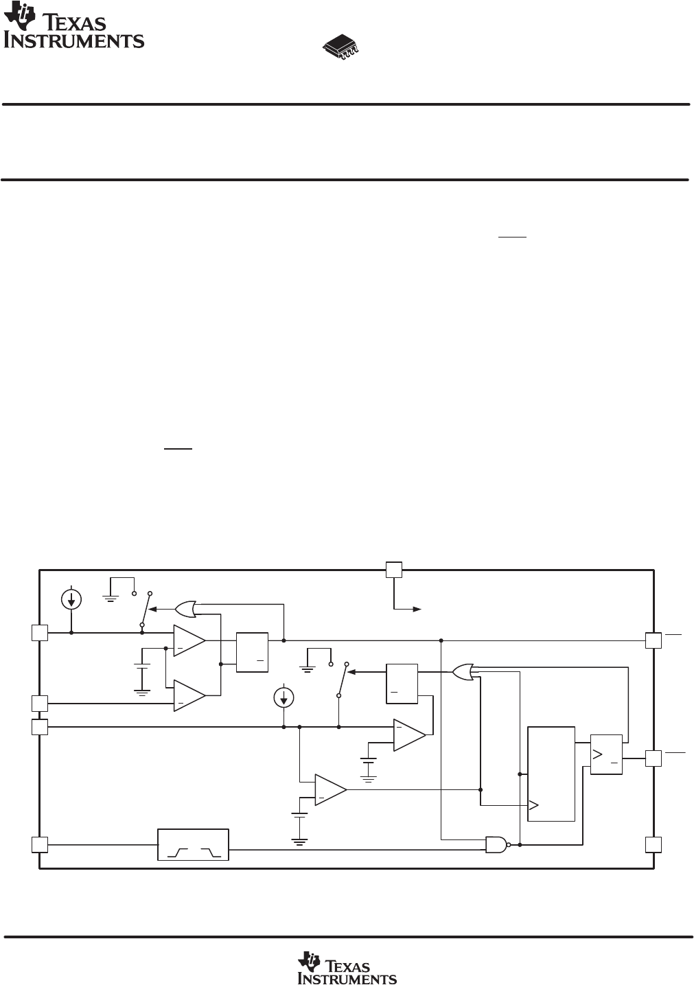
DESCRIPTION
The UCCx946 is designed to provide accurate
microprocessor supervision, including reset and
watchdog functions. During power up, the device
asserts a reset signal RES
with VDD as low as 1 V.
The reset signal remains asserted until the VDD
voltage rises and remains above the reset
threshold for the reset period. Both reset threshold
and reset period are programmable by the user.
The UCCx946 is also resistant to glitches on the
VDD line. Once RES
has been deasserted, any
drops below the threshold voltage need to be of
certain time duration and voltage magnitude to
generate a reset signal. These values are shown
in Figure 1. An I/O line of the microprocessor may
be tied to the watchdog input (WDI) for watchdog
functions. If the I/O line is not toggled within a set
watchdog period, programmable by the user,
WDO is asserted. The watchdog function is
disabled during reset conditions.
The UCCx946 is available in 8-pin SOIC(D), 8-pin
PDIP (N) and 8-pin TSSOP(PW) packages to
optimize board space.
UDG−0219
2
6
7
WDI
WP
8
VDD
3
5
POWER TO
CIRCUITRY
A3
A2
A1
A0
CLK
CLR
8−BIT
COUNTER
400 nA
WDO
GND
EDGE DETECT
WATCHDOG
TIMING
100 mV
1.235 V
2
RTH
4
RP
400 nA
POWER ON RESET
RES
+
+
S Q
QR
SQ
QR
SQ
QR
1
1.235 V
+
+
+
+
+
    !"#   $"%&! '#(
'"! !  $#!! $# )# #  #* "#
'' +,( '"! $!#- '#  #!#&, !&"'#
#-  && $##(
Copyright 2007, Texas Instruments Incorporated


SLUS247F − APRIL 1997 − REVISED NOVEMBER 2007
2
www.ti.com
ORDERING INFORMATION
T
A
PACKAGED DEVICES
(3)
T
A
(D) (N) (PW)
−40°C to 95°C UCC2946D UCC2946N UCC2946PW
0°C to 70°C UCC3946D UCC3946N UCC3946PW
(1)
The D and PW packages are also available taped and reeled. Add an R suffix to the device type (i.e., UCC2946DR) for quantities of 3,000
devices per reel.
These devices have limited built-in ESD protection. The leads should be shorted together or the device placed in conductive foam
during storage or handling to prevent electrostatic damage to the MOS gates.
ABSOLUTE MAXIMUM RATINGS
over operating free-air temperature range unless otherwise noted
(1)
UCC2946
UCC3946
UNIT
Input voltage range, V
IN
10 V
Junction temperature range, T
J
−55 to 150
Storage temperature, T
stg
−65 to 150
°C
Lead temperature 1,6 mm (1/16 inch) from case for 10 seconds 300
C
(1)
Stresses beyond those listed under “absolute maximum ratings” may cause permanent damage to the device. These are stress ratings only,
and functional operation of the device at these or any other conditions beyond those indicated under “recommended operating conditions” is
not implied. Exposure to absolute-maximum-rated conditions for extended periods may affect device reliability. Voltages are with respect to
GND. Currents are positive into, and negative out of the specified terminal.
1
2
3
4
8
7
6
5
GND
RTH
RES
RP
VDD
WDI
WP
WDO
D PACKAGE
(TOP VIEW)
TERMINAL FUNCTIONS
TERMINAL
I/O
DESCRIPTION
NAME NO.
I/O
DESCRIPTION
GND 1 Ground reference for the device
RES 3 O
This pin is high only if the voltage on the RTH has risen above 1.235 V. Once RTH rises above the threshold, this
pin remains low for the reset period. This pin asserts low and remains low if the RTH voltage dips below 1.235 V for
an amount of time determined by Figure 1.
RTH 2 I
This input compares its voltage to an internal 1.25-V reference. By using external resistors, a user can program any
desired reset threshold.
RP 4 I This pin allows the user to program the reset period by adjusting an external capacitor.
VDD 8 I Supply voltage for the device.
WDI 7 I
This pin is the input to the watchdog timer. If this pin is not toggled or strobed within the watchdog period, WDO is
asserted.
WDO 5 O
This pin is the watchdog output. This pin is asserted low if the WDI pin is not strobed or toggled within the watchdog
period.
WP 6 I This pin allows the user to program the watchdog period by adjusting an external capacitor.


SLUS247F − APRIL 1997 − REVISED NOVEMBER 2007
3
www.ti.com
ELECTRICAL CHARACTERISTICS
T
A
= 0°C to 70°C and 2.0 V V
DD
5.5 V for the UCC3946, T
A
= −40°C to 95°C and 2.1 V V
DD
5.5 V for the UCC2946, (unless
otherwise noted)
PARAMETER
TEST CONDITIONS MIN TYP MAX UNIT
REFERENCE
V
DD
UCC2946 2.1 5.5
V
V
DD
Operating voltage
UCC3946
2.0 5.5
V
I
DD
UCC2946 12 18
A
I
DD
Supply current
UCC3946
10 18
µA
V
DD(min)
UCC2946 1.1
V
V
DD(min)
Minimum operating voltage
UCC3946 1.0
V
RESET SECTION
UCC2946
1.170 1.235 1.260
V
Reset threshold voltage
UCC3946
V
DD
rising
1.190 1.235 1.260
V
Threshold hysteresis 15 mV
I
LEAK
Input leakage current 5 nA
V
OH
High-level output voltage I
SOURCE
= 2 mA V
DD
−0.3
I
SINK
= 2 mA 0.1
V
V
OL
UCC2946
0.4
V
V
OL
Low-level output voltage
UCC3946
I
SINK
= 20 µA, VDD = 1 V
0.2
VDD-to-output delay time VDD = −1 mV/µs 120 µs
UCC2946
140 200 320
ms
Reset period
UCC3946
C
RP
= 64 nF
160 200 260
ms
WATCHDOG SECTION
V
IH
High-level input voltage, WDI 0.7×V
DD
V
V
IL
Low-level input voltage, WDI 0.3×V
DD
V
UCC2946
0.96 1.60 2.56
s
Watchdog period
UCC3946
C
RP
= 64 nF
1.12 1.60 2.08
s
Watchdog pulse width 50 ns
V
OH
High-level output voltage I
SOURCE
= 2 mA V
DD
−0.3
V
V
OL
Low-level output voltage I
SINK
= 2 mA 0.1
V
(1)
Minimum supply voltage where RES
is considered valid.
123456NEXT