4
UC1846/7
UC2846/7
UC3846/7
Note 2. These parameters, although guaranteed over the recommended operating conditions, are not 100% tested in production.
Note 3. Parameter measured at trip point of latch with VPIN 5 = VREF, VPIN 6 = 0V.
Note 4. Amplifier gain defined as:
G
V
V
PIN
PIN
=
∆
∆
7
4
;
V
PIN4
= 0 to 1.0V
Note 5. Applies to UC1846/UC2846/UC3846 only due to polarity of outputs.
Note 6. Current into Pin 1 guaranteed to latch circuit in shutdown state.
Note 7. Current into Pin 1 guaranteed not to latch circuit in shutdown state.
UC1846/UC1847
UC3846/UC3847
PARAMETER TEST CONDITIONS UC2846/UC2847
MIN. TYP. MAX. MIN. TYP. MAX. UNITS
Shutdown Terminal Section (cont.)
Maximum Non-Latching (Note 7)
Current (I
PIN 1) 1.5 0.8 1.5 0.8 mA
Delay to Outputs T
J=25°C (Note 2) 300 600 300 600 ns
Output Section
Collector-Emitter Voltage 40 40 V
Collector Leakage Current V
C=40V (Note 5) 200 200 µA
Output Low Level I
SINK=20mA 0.1 0.4 0.1 0.4 V
I
SINK=100mA 0.4 2.1 0.4 2.1 V
Output High Level I
SOURCE=20mA 13 13.5 13 13.5 V
I
SOURCE=100mA 12 13.5 12 13.5 V
Rise Time C
L=1nF, TJ=25°C (Note 2) 50 300 50 300 ns
Fall Time C
L=1nF, TJ=25°C (Note 2) 50 300 50 300 ns
Under-Voltage Lockout Section
Start-Up Threshold 7.7 8.0 7.7 8.0 V
Threshold Hysteresis 0.75 0.75 V
Total Standby Current
Supply Current 17 21 17 21 mA
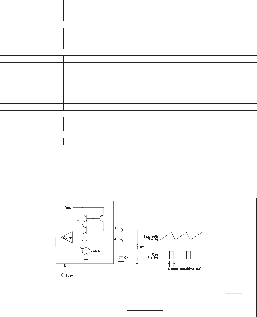
Oscillator Circuit
Output deadtime is determined by the external capacitor, C
T
, according to the formula:
τµ µ
Ω
ds Tf
() ()=
145C
ID
ID -
3.6
RT (k )
.
For large values of R
T
:
τµ µ
ds Tf
() ()≈
145C
.
Oscillator frequency is approximated by the formula:
fT kHz
RT k CT f
()
() ()
≈
•
2.2
Ωµ
.
ELECTRICAL
CHARACTERISTICS (cont.)
(Unless otherwise stated, these specifications apply for TA=-55°C to +125°C for UC1846/7;
-40°C to +85°C for the UC2846/7; and 0°C to +70°C for the UC3846/7; V
IN=15V, RT=10k,
C
T=4.7nF, TA=TJ.)
APPLICATIONS DATA
I
D
= Oscillator discharge current at 25°C is typically 7.5.


