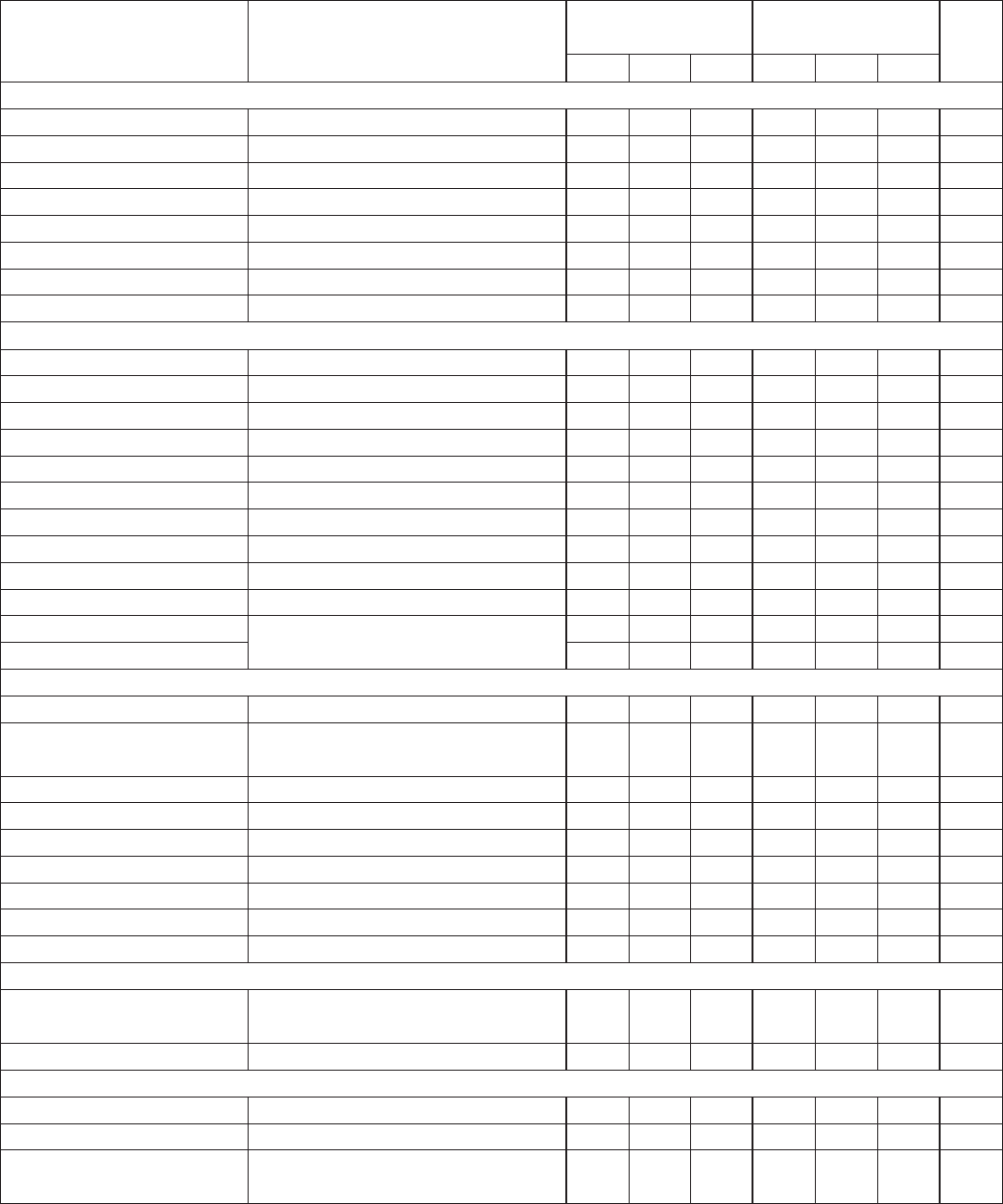
3
UC1846/7
UC2846/7
UC3846/7
UC1846/UC1847
UC3846/UC3847
PARAMETER TEST CONDITIONS UC2846/UC2847
MIN. TYP. MAX. MIN. TYP. MAX. UNITS
Oscillator Section
Initial Accuracy T
J=25°C 39 43 47 39 43 47 kHz
Voltage Stability V
IN=8V to 40V -1 2 -1 2 %
Temperature Stability Over Operating Range (Note 2) -1 -1 %
Sync Output High Level 3.9 4.35 3.9 4.35 V
Sync Output Low Level 2.3 2.5 2.3 2.5 V
Sync Input High Level Pin 8=0V 3.9 3.9 V
Sync Input Low Level Pin 8=0V 2.5 2.5 V
Sync Input Current Sync Voltage=3.9V, Pin 8=0V 1.3 1.5 1.3 1.5 mA
Error Amp Section
Input Offset Voltage 0.5 5 0.5 10 mV
Input Bias Current -0.6 -1 -0.6 -2 µA
Input Offset Current 40 250 40 250 nA
Common Mode Range V
IN=8V to 40V 0 VIN-2V 0 VIN-2V V
Open Loop Voltage Gain ∆V
O=1.2 to 3V, VCM=2V 80 105 80 105 dB
Unity Gain Bandwidth T
J=25°C (Note 2) 0.7 1.0 0.7 1.0 MHz
CMRR V
CM
=0V to 38V, VIN=40V 75 100 75 100 dB
PSRR V
IN=8V to 40V 80 105 80 105 dB
Output Sink Current V
ID=-15mV to -5V, VPIN 7=1.2V 2 6 2 6 mA
Output Source Current V
ID=15mV to 5V, VPIN 7=2.5V -0.4 -0.5 -0.4 -0.5 mA
High Level Output Voltage R
L=(Pin 7) 15kΩ 4.3 4.6 4.3 4.6 V
Low Level Output Voltage 0.7 1 0.7 1 V
Current Sense Amplifier Section
Amplifier Gain V
PIN 3=0V, Pin 1 Open (Notes 3 & 4) 2.5 2.75 3.0 2.5 2.75 3.0 V
Maximum Differential Input Pin 1 Open (Note 3)
Signal (V
PIN 4-VPIN 3)RL (Pin 7)=15kW 1.1 1.2 1.1 1.2 V
Input Offset Voltage V
PIN 1=0.5V, Pin 7 Open (Note 3) 5 25 5 25 mV
CMRR V
CM=1V to 12V 60 83 60 83 dB
PSRR V
IN=8V to 40V 60 84 60 84 dB
Input Bias Current V
PIN 1=0.5V, Pin 7 Open (Note 3) -2.5 -10 -2.5 -10 µA
Input Offset Current V
PIN 1=0.5V, Pin 7 Open (Note 3) 0.08 1 0.08 1 µA
Input Common Mode Range 0 V
IN-3 0 VIN-3 V
Delay to Outputs T
J=25°C, (Note 2) 200 500 200 500 ns
Current Limit Adjust Section
Current Limit Offset V
PIN 3=0V, VPIN 4=0V, Pin 7 Open
(Note 3) 0.45 0.5 0.55 0.45 0.5 0.55 V
Input Bias Current V
PIN 5=VREF,VPIN 6=0V -10 -30 -10 -30 µA
Shutdown Terminal Section
Threshold Voltage 250 350 400 250 350 400 mV
Input Voltage Range 0 V
IN 0VIN V
Minimum Latching Current (Note 6)
(I
PIN 1) 3.0 1.5 3.0 1.5 mA
ELECTRICAL
CHARACTERISTICS (cont.)
(Unless otherwise stated, these specifications apply for TA=-55°C to +125°C for UC1846/7;
-40°C to +85°C for the UC2846/7; and 0°C to +70°C for the UC3846/7; V
IN=15V, RT=10k,
C
T=4.7nF, TA=TJ.)


