Closed Dec 25th-26th
800-300-1968
We Stock Hard to Find Parts
My Account
|
My Orders
|
My Cart
Questions?
(800) 300-1968
Register
(current)
My Account
(current)
My Orders
(current)
My Cart
(current)
Categories
(current)
Manufacturers
Request a Quote
Sell Your Excess
Consignment
Quality Assurance
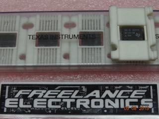
UC1845J
Part #
UC1845J
Description
CUR MODE PWM CONTROLLERBIPOLAR, 8 PIN CDIP
Category
IC
Availability
In Stock
Qty
1
Qty
Price
1 +
$30.43969
Manufacturer
Available
Qty
UNITRODE
Date Code: 9927
Freelance Stock:
1
Ships Immediately
Add to Cart
Related Items
Texas Instruments
IC
UC1842
$7.26511
UNITRODE
IC
UC1842J/883BC
$24.35176
UNITRODE
IC
UC1843AJ
$11.39429
UNITRODE
IC
UC1843J
$6.71153
UNITRODE
IC
UC1843J/883B
$33.21047
Texas Instruments
IC
UC1843W
$8.00400