Closed Dec 25th-26th
800-300-1968
We Stock Hard to Find Parts
My Account
|
My Orders
|
My Cart
Questions?
(800) 300-1968
Register
(current)
My Account
(current)
My Orders
(current)
My Cart
(current)
Categories
(current)
Manufacturers
Request a Quote
Sell Your Excess
Consignment
Quality Assurance
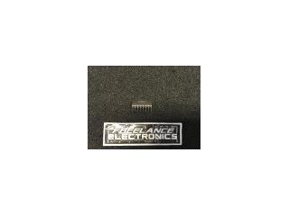
UC1524AJ
Part #
UC1524AJ
Description
PULSE WIDTH MODULATER16 PIN CDIP
Category
IC
Availability
Out of Stock
Qty
0
Qty
Price
1 +
$6.40210
Related Items
UNITRODE
IC
UC1525AJ
$55.50276
UNITRODE
IC
UC1525AJ/883BC
UNITRODE
IC
UC1525BJ/883BC
$24.35176
UNITRODE
IC
UC1526AJ
$11.26269
UNITRODE
IC
UC1526AJ/883B
$21.91659
UNITRODE
IC
UC1526AJ/883BC
$28.92990