Freelance Electronics Components Distributor
Closed Dec 25th-26th
800-300-1968
We Stock Hard to Find Parts

TUSB3200ACPAH

Part # TUSB3200ACPAH
Description USB STREAMING CONTROLLER
Category IC
Availability Out of Stock
Qty 0
Qty Price
1 + $6.01940


Technical Document


DISCLAIMER: The information provided herein is solely for informational purposes. Customers must be aware of the suitability of this product for their application, and consider that variable factors such as Manufacturer, Product Category, Date Codes, Pictures and Descriptions may differ from available inventory.

3–3
3.4 Timing Characteristics
3.4.1 Clock and Control Signals Over Recommended Operating Conditions
(unless otherwise noted)
PARAMETER TEST CONDITIONS MIN TYP MAX UNITS
f
MCLKO
Clock frequency, MCLKO C
L
= 50 pF, See Note 1 1 25 MHz
f
MCLKO2
Clock frequency, MCLKO2 C
L
= 50 pF, See Note 1 1 25 MHz
f
MCLKI
Clock frequency, MCLKI See Note 1 5 25 MHz
f
MCLKI2
Clock frequency, MCLKI2 See Note 1 5 25 MHz
t
w(L)
Pulse duration, XINT low C
L
= 50 pF 0.2 10 µs
NOTE 1: Worst case duty cycle is 45/55.
t
w(L)
XINT
Figure 3–1. External Interrupt Timing Waveform
3.4.2 USB Transceiver Signals Over Recommended Operating Conditions
(unless otherwise noted)
PARAMETER TEST CONDITIONS MIN TYP MAX UNITS
t
r
Transition rise time for DP or DM 4 20 ns
t
f
Transition fall time for DP or DM 4 20 ns
t
RFM
Rise/fall time matching (t
r
/t
f
) × 100 90% 110%
V
O(CRS)
Voltage output signal crossover 1.3 2 V
t
r
, t
f
90%
10%
V
O(CRS)
V
OH
V
OL
DM
DP
Figure 3–2. USB Differential Driver Timing Waveform
3–4
3.4.3 CODEC Port Interface Signals (AC ’97 Modes), T
A
= 25°C, DV
DD
= 3.3 V, DV
DSS
= 5 V,
AV
DD
= 3.3 V
PARAMETER TEST CONDITIONS MIN TYP MAX UNITS
f
BIT_CLK
Frequency, BIT_CLK See Note 1 12.288 MHz
t
cyc1
Cycle time, BIT_CLK See Note 1 81.4 ns
t
w1(H)
Pulse duration, BIT_CLK high See Note 1 36 40.7 45 ns
t
w1(L)
Pulse duration, BIT_CLK low See Note 1 36 40.7 45 ns
f
SYNC
Frequency, SYNC C
L
= 50 pF 48 kHz
t
cyc2
Cycle time, SYNC C
L
= 50 pF 20.8 µs
t
w2(H)
Pulse duration, SYNC high C
L
= 50 pF 1.3 µs
t
w2(L)
Pulse duration, SYNC low C
L
= 50 pF 19.5 µs
t
pd1
Propagation delay time, BIT_CLK rising edge to SYNC, SD_OUT
and RESET
C
L
= 50 pF 15 ns
t
su
Setup time, SD_IN to BIT_CLK falling edge 10 ns
t
h
Hold time, SD_IN from BIT_CLK falling edge 10 ns
NOTE 1: Worst case duty cycle is 45/55.
t
w1(H)
t
w1(L)
t
cyc1
t
w2(H)
t
w2(L)
t
cyc2
BIT_CLK
SYNC
Figure 3–3. BIT_CLK and SYNC Timing Waveforms
t
su
t
h
BIT_CLK
t
pd1
SYNC, SD_OUT, RESET
SD_IN
Figure 3–4. SYNC, SD_IN, and SD_OUT Timing Waveforms
3–5
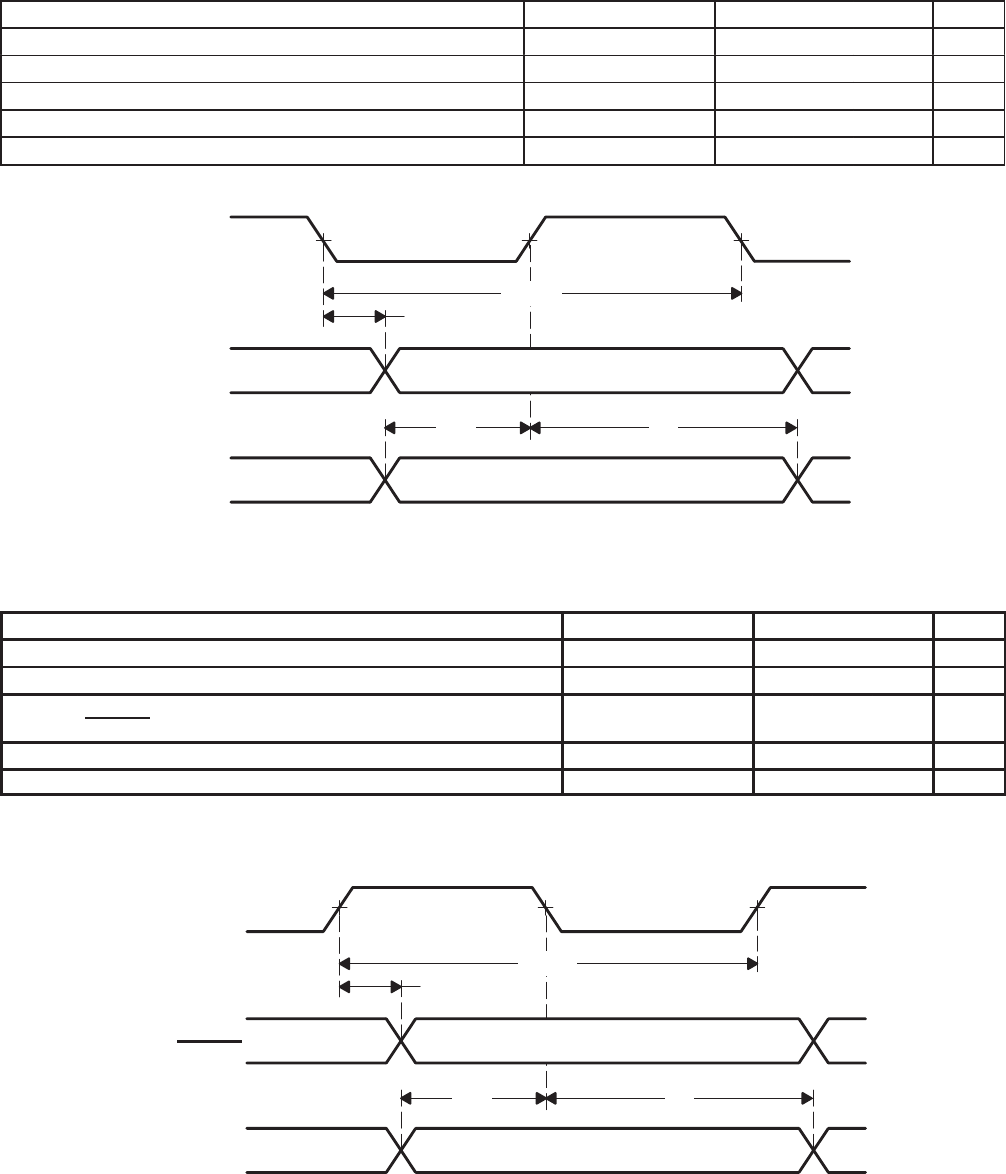
3.4.4 CODEC Port Interface Signals (I
2
S Modes) Over Recommended Operating Conditions
(unless otherwise noted)
PARAMETER TEST CONDITIONS MIN TYP MAX UNITS
f
SCLK
Frequency, SCLK C
L
= 50 pF (32)F
S
(64)F
S
MHz
t
cyc
Cycle time, SCLK C
L
= 50 pF, See Note 1 1/(64)F
S
1/(32)F
S
ns
t
pd
Propagation delay, SCLK falling edge to LRCLK and SDOUT C
L
= 50 pF 15 ns
t
su
Setup time, SDIN to SCLK rising edge 10 ns
t
h
Hold time, SDIN from SCLK rising edge 10 ns
NOTE 1: Worst case duty cycle is 45/55.
t
su
t
h
SCLK
LRCLK, SD_OUT
SD_IN
t
pd
t
cyc
Figure 3–5. I
2
S Mode Timing Waveforms
3.4.5 CODEC Port Interface Signals (General Purpose Mode) Over Recommended Operating
Conditions (unless otherwise noted)
PARAMETER TEST CONDITIONS MIN TYP MAX UNITS
f
CSCLK
Frequency, CSCLK C
L
= 50 pF 0.125 25 MHz
t
cyc
Cycle time, CSCLK C
L
= 50 pF, See Note 2 0.040 8 µs
t
pd
Propagation delay, CSCLK to CSYNC, CDATO, CSCHNE and
CRESET
C
L
= 50 pF 15 ns
t
su
Setup time, CDATI to CSCLK 10 ns
t
h
Hold time, CDATI from CSCLK 10 ns
NOTE 2: The timing waveforms in Figure 3-6 show the CSYNC, CDATO, CSCHNE and CRESET signals generated with the rising edge of the
clock and the CDATI signal sampled with the falling edge of the clock. The edge of the clock used is programmable. However, the timing
characteristics are the same regardless of which edge of the clock is used.
t
su
t
h
CSCLK
CSYNC, CDATO,
CSCHNE, CRESET
CDATI
t
pd
t
cyc
Figure 3–6. General-Purpose Mode Timing Waveforms
PREVIOUS89101112131415161718192021NEXT