3–1
3 Electrical Specifications
3.1 Absolute Maximum Ratings Over Operating Temperature Ranges (unless
otherwise noted)
†
Supply voltage range, DV
DD
–0.5 to 3.6 V. . . . . . . . . . . . . . . . . . . . . . . . . . . . . . . . . . . . . . . . . . . . . . . . . . . . . . . .
DV
DDS
–0.5 to 5.5 V. . . . . . . . . . . . . . . . . . . . . . . . . . . . . . . . . . . . . . . . . . . . . . . . . . . . . . .
AV
DD
–0.5 to 3.6 V. . . . . . . . . . . . . . . . . . . . . . . . . . . . . . . . . . . . . . . . . . . . . . . . . . . . . . . .
Input voltage range, V
I
: 3.3-V TTL/LVCMOS –0.5 V to DV
DD
+ 0.5 V. . . . . . . . . . . . . . . . . . . . . . . . . . . . . . . . .
5-V Compatible –0.5 V to DV
DDS
+ 0.5 V. . . . . . . . . . . . . . . . . . . . . . . . . . . . . . . . . . .
5-V–3.3-V TTL level shifting –0.5 V to DV
DDS
+ 0.5 V. . . . . . . . . . . . . . . . . . . . . . . .
Output voltage range, V
O
: 3.3-V TTL/LVCMOS –0.5 V to DV
DD
+ 0.5 V. . . . . . . . . . . . . . . . . . . . . . . . . . . . . . .
5-V Compatible –0.5 V to DV
DDS
+ 0.5 V. . . . . . . . . . . . . . . . . . . . . . . . . . . . . . . . .
3.3-V–5-V TTL level shifting –0.5 V to DV
DDS
+ 0.5 V. . . . . . . . . . . . . . . . . . . . . .
3.3-V–5-V CMOS level shifting –0.5 V to DV
DDS
+ 0.5 V. . . . . . . . . . . . . . . . . . . .
Input clamp current, I
IK
(V
I
< 0 or V
I
> DVDD) ±20 mA. . . . . . . . . . . . . . . . . . . . . . . . . . . . . . . . . . . . . . . . . . . . . .
Output clamp current, I
OK
(V
O
< 0 or V
O
> DVDD) ±20 mA. . . . . . . . . . . . . . . . . . . . . . . . . . . . . . . . . . . . . . . . . .
Storage temperature range, T
stg
–65°C to 150°C. . . . . . . . . . . . . . . . . . . . . . . . . . . . . . . . . . . . . . . . . . . . . . . . . .
†
Stresses beyond those listed under “absolute maximum ratings” may cause permanent damage to the device. These are stress ratings only and
functional operation of the device at these or any other conditions beyond those indicated under “recommended operating conditions” is not
implied. Exposure to absolute-maximum-rated conditions for extended periods may affect device reliability.
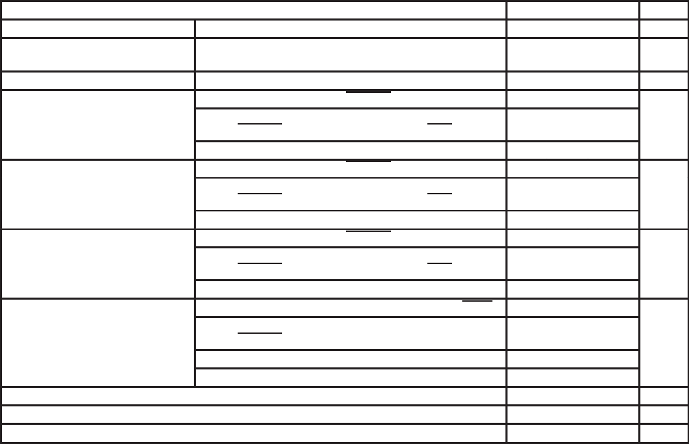
3.2 Recommended Operating Conditions
MIN NOM MAX UNITS
Digital supply voltage, DV
DD
3 3.3 3.6 V
Secondary digital supply voltage,
DV
DDS
4.5 5 5.5 V
Analog supply voltage, AV
DD
3 3.3 3.6 V
3.3-V TTL/LVCMOS (EXTEN, MRESET, TEST) 2 DV
DD
High-level input voltage, V
IH
5-V compatible TTL/LVCMOS (CSCLK, CSYNC, CDATO,
CDATI, CRESET
, CSCHNE, P1, P3, PLLOEN, XINT)
2 DV
DDS
V
5-V – 3.3-V TTL level shifting (MCLKI, MCLKI2, SDA) 2 DV
DDS
3.3-V TTL/LVCMOS (EXTEN, MRESET, TEST) 0 0.8
Low-level input voltage, V
IL
5-V compatible TTL/LVCMOS (CSCLK, CSYNC, CDATO,
CDATI, CRESET
, CSCHNE, P1, P3, PLLOEN, XINT)
0 0.8
V
5-V – 3.3-V TTL level shifting (MCLKI, MCLKI2, SDA) 0 0.8
3.3-V TTL/LVCMOS (EXTEN, MRESET, TEST) 0 DV
DD
Input voltage, V
I
5-V compatible TTL/LVCMOS (CSCLK, CSYNC, CDATO,
CDATI, CRESET
, CSCHNE, P1, P3, PLLOEN, XINT)
0 DV
DDS
V
5-V – 3.3-V TTL level shifting (MCLKI, MCLKI2, SDA) 0 DV
DDS
3.3-V TTL/LVCMOS (MCLKO, MCLKO2, PLLO, PUR, RSTO) 0 DV
DD
Output voltage, V
5-V compatible TTL/LVCMOS (CSCLK, CSYNC, CDATO,
CDATI, CRESET
, CSCHNE, P1, P3)
0 DV
DD
V
3.3-V – 5-V TTL level shifting, open drain (SCL, SDA) 0 DV
DDS
3.3-V – 5-V CMOS level shifting (PWMO) 0 DV
DDS
Input transition time, t
t
(t
r
and t
f
, 10% to 90%) 0 6 ns
Operating ambient air temperature range, T
A
0 25 70 °C
Operating junction temperature range, T
J
0 25 115 °C


