Freelance Electronics Components Distributor
Closed Dec 25th-26th
800-300-1968
We Stock Hard to Find Parts

TSB12LV26TPZEP

Part # TSB12LV26TPZEP
Description V62/03627-01XE -OHCI-LYNX PCI-BASED - Trays
Category IC
Availability In Stock
Qty 2
Qty Price
1 + $10.15828
Manufacturer Available Qty
Texas Instruments
Date Code: 0336
  • Shipping Freelance Stock: 2
    Ships Immediately


Technical Document


DISCLAIMER: The information provided herein is solely for informational purposes. Customers must be aware of the suitability of this product for their application, and consider that variable factors such as Manufacturer, Product Category, Date Codes, Pictures and Descriptions may differ from available inventory.

2−3
Table 2−2. Signal Names Sorted Alphanumerically to Terminal Number
TERMINAL NAME NO. TERMINAL NAME NO. TERMINAL NAME NO. TERMINAL NAME NO.
CYCLEIN 78 PCI_AD11 59 PCI_CLK 12 PHY_DATA7 81
CYCLEOUT 77 PCI_AD12 58 PCI_CLKRUN 7 PHY_LINKON 98
GND 1 PCI_AD13 57 PCI_DEVSEL 47 PHY_LPS 99
GND 11 PCI_AD14 56 PCI_FRAME 43 PHY_LREQ 97
GND 24 PCI_AD15 54 PCI_GNT 14 PHY_SCLK 95
GND 30 PCI_AD16 40 PCI_IDSEL 29 REG_EN 79
GND 50 PCI_AD17 38 PCI_INTA 8 REG18 42
GND 60 PCI_AD18 37 PCI_IRDY 44 REG18 100
GND 75 PCI_AD19 36 PCI_PAR 52 SCL 4
GND 83 PCI_AD20 34 PCI_PERR 49 SDA 5
GND 94 PCI_AD21 33 PCI_PME 17 V
CCP
6
GPIO2 2 PCI_AD22 32 PCI_REQ 15 V
CCP
16
GPIO3 3 PCI_AD23 31 PCI_RST 76 V
CCP
39
G_RST 10 PCI_AD24 27 PCI_SERR 51 V
CCP
63
PCI_AD0 74 PCI_AD25 26 PCI_STOP 48 V
CCP
87
PCI_AD1 73 PCI_AD26 25 PCI_TRDY 45 3.3 V
CC
9
PCI_AD2 72 PCI_AD27 23 PHY_CTL0 93 3.3 V
CC
13
PCI_AD3 71 PCI_AD28 22 PHY_CTL1 92 3.3 V
CC
20
PCI_AD4 69 PCI_AD29 21 PHY_DATA0 90 3.3 V
CC
35
PCI_AD5 68 PCI_AD30 19 PHY_DATA1 89 3.3 V
CC
46
PCI_AD6 67 PCI_AD31 18 PHY_DATA2 88 3.3 V
CC
55
PCI_AD7 66 PCI_C/BE0 65 PHY_DATA3 86 3.3 V
CC
70
PCI_AD8 64 PCI_C/BE1 53 PHY_DATA4 85 3.3 V
CC
80
PCI_AD9 62 PCI_C/BE2 41 PHY_DATA5 84 3.3 V
CC
91
PCI_AD10 61 PCI_C/BE3 28 PHY_DATA6 82 3.3 V
CC
96
The terminals in Table 2−3 through Table 2−8 are grouped in tables by functionality, such as PCI system function
and power supply function. The terminal numbers are also listed for convenient reference.
Table 2−3. Power Supply Terminals
TERMINAL
I/O
DESCRIPTION
NAME NO.
I/O
DESCRIPTION
GND
1, 11, 24, 30,
50, 60, 75, 83,
94
I Device ground terminals
V
CCP
6, 16, 39, 63,
87
I PCI signaling clamp voltage power input. PCI signals are clamped per the PCI Local Bus Specification.
3.3 V
CC
9, 13, 20, 35,
46, 55, 70, 80,
91, 96
I 3.3-V power supply terminals
2−4
Table 2−4. PCI System Terminals
TERMINAL
I/O
DESCRIPTION
NAME NO.
I/O
DESCRIPTION
G_RST 10 I
Global power reset. This reset brings all of the TSB12LV26 internal registers to their default states, including
those registers not reset by PCI_RST
. When G_RST is asserted, the device is completely nonfunctional.
When implementing wake capabilities from the 1394 host controller, it is necessary to implement two resets
to the TSB12LV26 device. G_RST
is designed to be a one-time power-on reset, and PCI_RST must be
connected to the PCI bus RST
. If wake capabilities are not required, G_RST can be connected to the PCI bus
RST
(see PCI_RST, terminal 76).
PCI_CLK 12 I
PCI bus clock. Provides timing for all transactions on the PCI bus. All PCI signals are sampled at rising edge
of PCI_CLK.
PCI_INTA 8 O
Interrupt signal. This output indicates interrupts from the TSB12LV26 device to the host. This terminal is
implemented as open-drain.
PCI_RST 76 I
PCI reset. When this bus reset is asserted, the TSB12LV26 device places all output buffers in a
high-impedance state and resets all internal registers except device power management context- and
vendor-specific bits initialized by host power-on software. When PCI_RST is asserted, the device is
completely nonfunctional.
If this terminal is implemented, it must be connected to the PCI bus RST
signal. Otherwise, it must be pulled
high to link V
CC
through a 4.7-k resistor, or strapped to the G_RST
terminal (see G_RST, terminal 10).
Table 2−5. PCI Address and Data Terminals
TERMINAL
I/O
NAME NO.
I/O
PCI_AD31
PCI_AD30
PCI_AD29
PCI_AD28
PCI_AD27
PCI_AD26
PCI_AD25
PCI_AD24
PCI_AD23
PCI_AD22
PCI_AD21
PCI_AD20
PCI_AD19
PCI_AD18
PCI_AD17
PCI_AD16
PCI_AD15
PCI_AD14
PCI_AD13
PCI_AD12
PCI_AD11
PCI_AD10
PCI_AD9
PCI_AD8
PCI_AD7
PCI_AD6
PCI_AD5
PCI_AD4
PCI_AD3
PCI_AD2
PCI_AD1
PCI_AD0
18
19
21
22
23
25
26
27
31
32
33
34
36
37
38
40
54
56
57
58
59
61
62
64
66
67
68
69
71
72
73
74
I/O
PCI address/data bus. These signals make up the multiplexed PCI address and data bus on the PCI interface.
During the address phase of a PCI cycle, AD31−AD0 contain a 32-bit address or other destination information.
During the data phase, AD31−AD0 contain data.
2−5
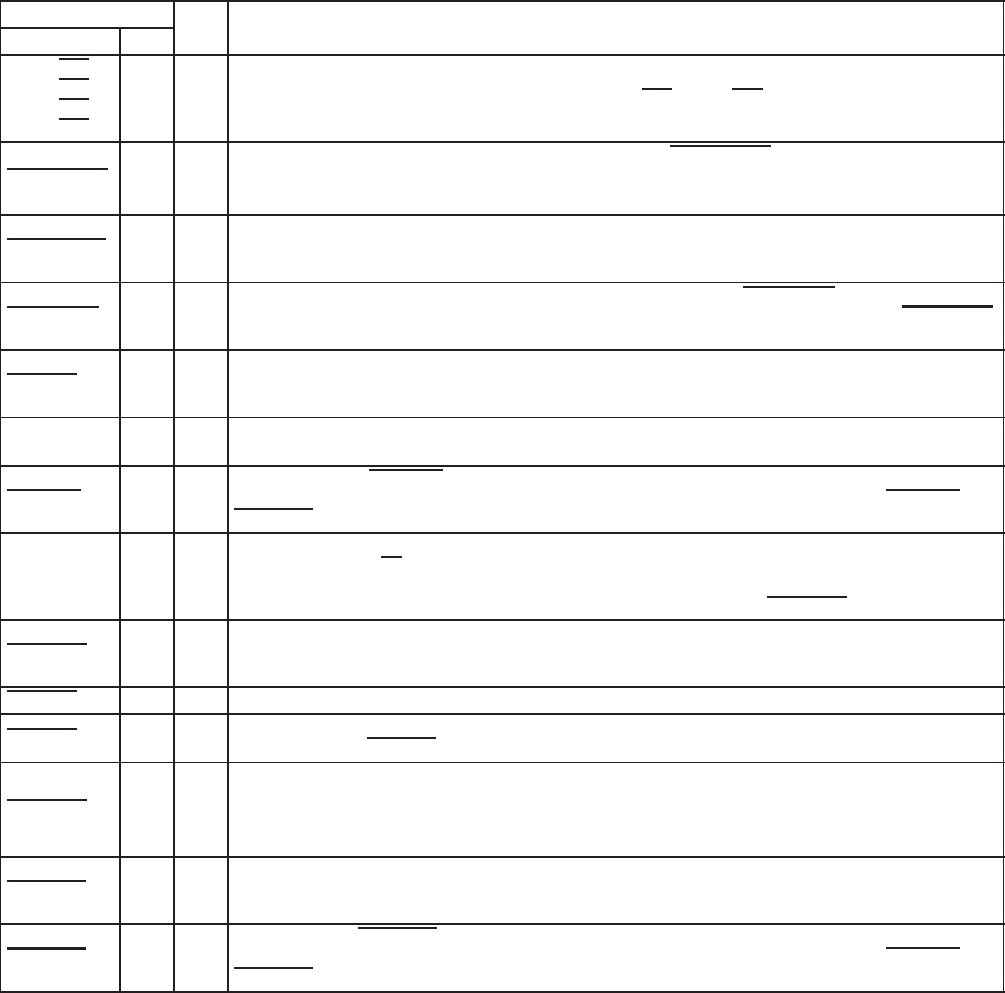
Table 2−6. PCI Interface Control Terminals
TERMINAL
I/O
DESCRIPTION
NAME NO.
I/O
DESCRIPTION
PCI_C/BE0
PCI_C/BE1
PCI_C/BE2
PCI_C/BE3
65
53
41
28
I/O
PCI bus commands and byte enables. The command and byte enable signals are multiplexed on the same PCI
terminals. During the address phase of a bus cycle PCI_C/BE3
−PCI_C/BE0 define the bus command. During
the data phase, this 4-bit bus is used as byte enables.
PCI_CLKRUN 7 I/O
Clock run. This terminal provides clock control through the PCI_CLKRUN protocol. An internal pulldown
resistor is implemented on this terminal.
This terminal is implemented as open-drain.
PCI_DEVSEL 47 I/O
PCI device select. The TSB12LV26 device asserts this signal to claim a PCI cycle as the target device. As a
PCI initiator, the TSB12LV26 device monitors this signal until a target responds. If no target responds before
time-out occurs, the TSB12LV26 device terminates the cycle with an initiator abort.
PCI_FRAME 43 I/O
PCI cycle frame. This signal is driven by the initiator of a PCI bus cycle. PCI_FRAME is asserted to indicate
that a bus transaction is beginning, and data transfers continue while this signal is asserted. When PCI_FRAME
is deasserted, the PCI bus transaction is in the final data phase.
PCI_GNT 14 I
PCI bus grant. This signal is driven by the PCI bus arbiter to grant the TSB12LV26 device access to the PCI
bus after the current data transaction has completed. This signal may or may not follow a PCI bus request,
depending upon the PCI bus parking algorithm.
PCI_IDSEL 29 I
Initialization device select. PCI_IDSEL selects the TSB12LV26 device during configuration space accesses.
PCI_IDSEL can be connected to one of the upper 24 PCI address lines on the PCI bus.
PCI_IRDY 44 I/O
PCI initiator ready. PCI_IRDY indicates the ability of the PCI bus initiator to complete the current data phase
of the transaction. A data phase is completed upon a rising edge of PCLK where both PCI_IRDY
and
PCI_TRDY
are asserted.
PCI_PAR 52 I/O
PCI parity. In all PCI bus read and write cycles, the TSB12LV26 device calculates even parity across the
PCI_AD and PCI_C/BE
buses. As an initiator during PCI cycles, the TSB12LV26 device outputs this parity
indicator with a one PCI_CLK delay. As a target during PCI cycles, the calculated parity is compared to the
initiator parity indicator; a miscompare can result in a parity error assertion (PCI_PERR).
PCI_PERR 49 I/O
PCI parity error indicator. This signal is driven by a PCI device to indicate that calculated parity does not match
PCI_PAR when PERR_ENB (bit 6) in the command register at offset 04h in the PCI configuration space (see
Section 3.4, Command Register) is set to 1.
PCI_PME 17 O Power management event. This terminal indicates wake events to the host.
PCI_REQ 15 O
PCI bus request. Asserted by the TSB12LV26 device to request access to the bus as an initiator. The host
arbiter asserts the PCI_GNT
signal when the TSB12LV26 device has been granted access to the bus.
PCI_SERR 51 O
PCI system error. When SERR_ENB (bit 8) in the command register at offset 04h in the PCI configuration space
(see Section 3.4, Command Register) is set to 1, the output is pulsed, indicating an address parity error has
occurred. The TSB12LV26 device need not be the target of the PCI cycle to assert this signal.
This terminal is implemented as open-drain.
PCI_STOP 48 I/O
PCI cycle stop signal. This signal is driven by a PCI target to request the initiator to stop the current PCI bus
transaction. This signal is used for target disconnects, and is commonly asserted by target devices which do
not support burst data transfers.
PCI_TRDY 45 I/O
PCI target ready. PCI_TRDY indicates the ability of the PCI bus target to complete the current data phase of
the transaction. A data phase is completed upon a rising edge of PCI_CLK where both PCI_IRDY
and
PCI_TRDY
are asserted.
PREVIOUS12345678910NEXT