4−6
4.3 Asynchronous Transmit Retries Register
The asynchronous transmit retries register indicates the number of times the TSB12LV26 device attempts a retry for
asynchronous DMA request transmit and for asynchronous physical and DMA response transmit. See Table 4−4 for
a complete description of the register contents.
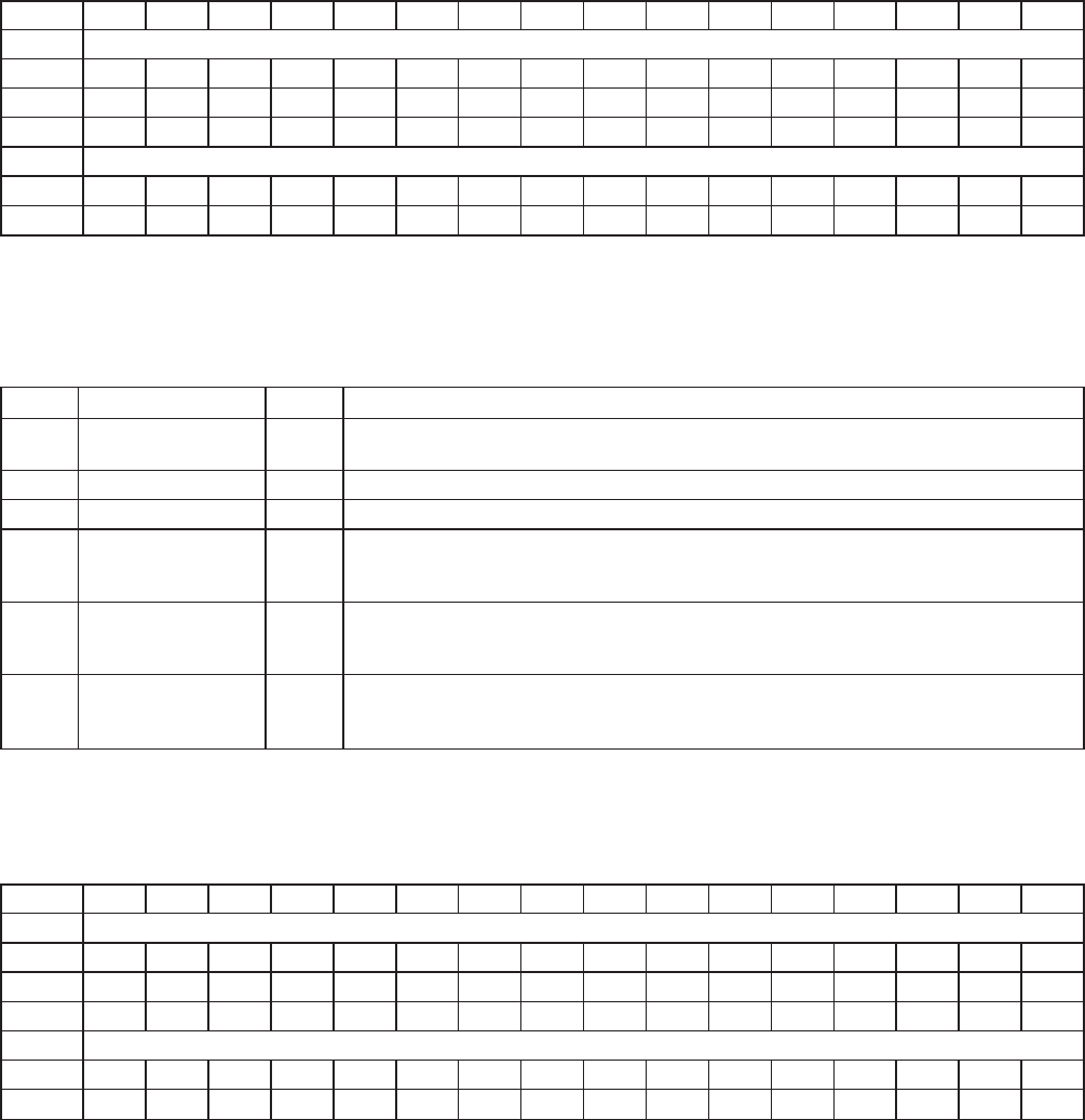
Bit 31 30 29 28 27 26 25 24 23 22 21 20 19 18 17 16
Name Asynchronous transmit retries
Type R R R R R R R R R R R R R R R R
Default 0 0 0 0 0 0 0 0 0 0 0 0 0 0 0 0
Bit 15 14 13 12 11 10 9 8 7 6 5 4 3 2 1 0
Name Asynchronous transmit retries
Type R R R R R/W R/W R/W R/W R/W R/W R/W R/W R/W R/W R/W R/W
Default 0 0 0 0 0 0 0 0 0 0 0 0 0 0 0 0
Register: Asynchronous transmit retries
Type: Read/Write, Read-only
Offset: 08h
Default: 0000 0000h
Table 4−4. Asynchronous Transmit Retries Register Description
BIT FIELD NAME TYPE DESCRIPTION
31−29 secondLimit R The second limit field returns 0s when read, because outbound dual-phase retry is not
implemented.
28−16 cycleLimit R The cycle limit field returns 0s when read, because outbound dual-phase retry is not implemented.
15−12 RSVD R Reserved. Bits 15−12 return 0s when read.
11−8 maxPhysRespRetries R/W The maxPhysRespRetries field tells the physical response unit how many times to attempt to retry
the transmit operation for the response packet when a busy acknowledge or ack_data_error is
received from the target node.
7−4 maxATRespRetries R/W The maxATRespRetries field tells the asynchronous transmit response unit how many times to
attempt to retry the transmit operation for the response packet when a busy acknowledge or
ack_data_error is received from the target node.
3−0 maxATReqRetries R/W The maxATReqRetries field tells the asynchronous transmit DMA request unit how many times
to attempt to retry the transmit operation for the response packet when a busy acknowledge or
ack_data_error is received from the target node.
4.4 CSR Data Register
The CSR data register accesses the bus-management CSR registers from the host through compare-swap
operations. This register contains the data to be stored in a CSR if the compare is successful.
Bit 31 30 29 28 27 26 25 24 23 22 21 20 19 18 17 16
Name CSR data
Type R R R R R R R R R R R R R R R R
Default X X X X X X X X X X X X X X X X
Bit 15 14 13 12 11 10 9 8 7 6 5 4 3 2 1 0
Name CSR data
Type R R R R R R R R R R R R R R R R
Default X X X X X X X X X X X X X X X X
Register: CSR data
Type: Read-only
Offset: 0Ch
Default: XXXX XXXXh


