Introduction
28
November 2002 − Revised January 2005SPRS205D
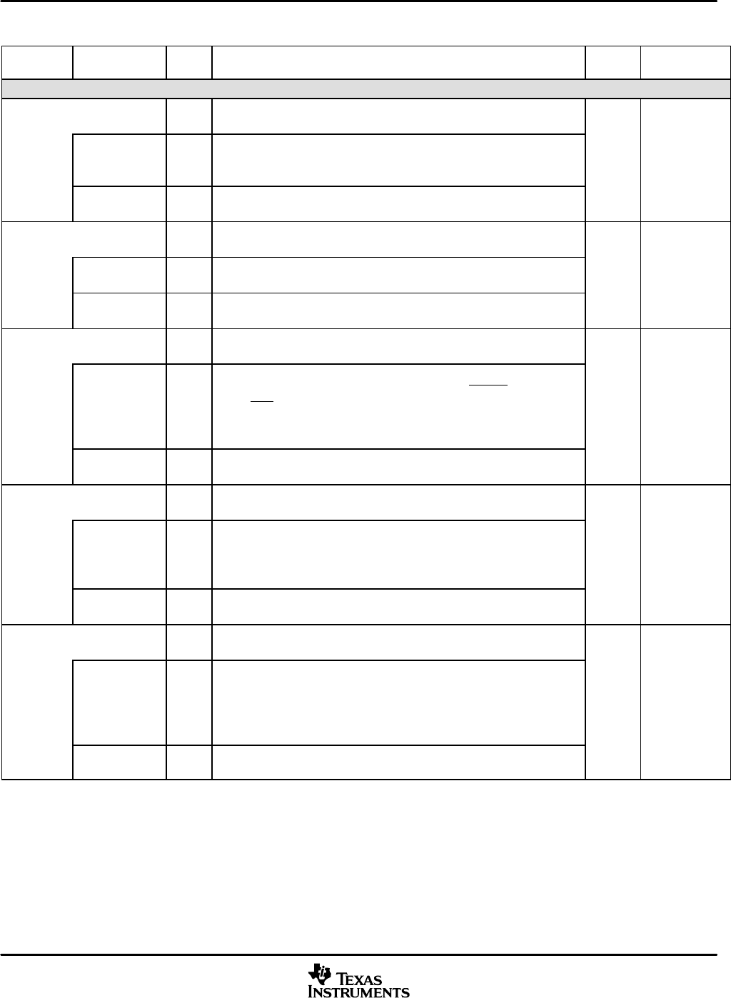
Table 2−3. Signal Descriptions (Continued)
TERMINAL
NAME
RESET
CONDITION
BK
‡
FUNCTIONI/O/Z
†
MULTIPLEXED
SIGNAL NAME
MULTICHANNEL BUFFERED SERIAL PORTS SIGNALS (CONTINUED)
S21 I/O/Z
McBSP2 data receive or Secure Digital2 data1. At reset, this pin is
configured as McBSP2.DR.
McBSP2.DR I
McBSP2 serial data receive. McBSP2.DR is selected when the External
Bus Selection Register has 00 in the Serial Port2 Mode bit field or following
reset.
Input
SD2.DAT1 I/O/Z
SD2 data1 is selected when the External Bus Selection Register has 10 in
the Serial Port2 Mode bit field.
S22 I/O/Z
McBSP2 receive frame synchronization or Secure Digital2 data2. At reset,
this pin is configured as McBSP2.FSR.
McBSP2.FSR I
McBSP2 receive frame synchronization. The McBSP2.FSR pulse initiates
the data receive process over McBSP2.DR.
Input
SD2.DAT2 I/O/Z
SD2 data2 is selected when the External Bus Selection Register has 10 in
the Serial Port2 Mode bit field.
S23 O/Z
McBSP2 data transmit or MultiMedia Card/Secure Digital2 serial clock. At
reset, this pin is configured as McBSP2.DX.
McBSP2.DX O/Z
McBSP2 serial data transmit. McBSP2.DX is placed in the
high-impedance state when not transmitting, when RESET is asserted, or
when OFF is low. McBSP2.DX is selected when the External Bus
Selection Register has 00 in the Serial Port2 Mode bit field or following
reset.
BK Hi-Z
MMC2.CLK
SD2.CLK
O
MMC2 or SD2 serial clock is selected when the External Bus Selection
Register has 10 in the Serial Port2 Mode bit field.
S24 I/O/Z
McBSP2 transmit clock or MultiMedia Card/Secure Digital2 data0. At
reset, this pin is configured as McBSP2.CLKX.
McBSP2.CLKX I/O/Z
McBSP2 transmit clock. McBSP2.CLKX serves as the serial shift clock for
the serial port transmitter. The McBSP2.CLKX pin is configured as input
after reset. McBSP2.CLKX is selected when the External Bus Selection
Register has 00 in the Serial Port2 Mode bit field or following reset.
H Input
MMC2.DAT
SD2.DAT0
I/O/Z
MMC2 or SD2 data0 pin is selected when the External Bus Selection
Register has 10 in the Serial Port2 Mode bit field.
S25 I/O/Z
McBSP2 transmit frame synchronization or Secure Digital2 data3. At
reset, this pin is configured as McBSP2.FSX.
McBSP2.FSX I/O/Z
McBSP2 frame synchronization. The McBSP2.FSX pulse initiates the
data transmit process over McBSP2.DX. McBSP2.FSX is configured as
an input following reset. McBSP2.FSX is selected when the External Bus
Selection Register has 00 in the Serial Port2 Mode bit field or following
reset.
Input
SD2.DAT3 I/O/Z
SD2 data3 is selected when the External Bus Selection Register has 10 in
the Serial Port2 Mode bit field.
†
I = Input, O = Output, S = Supply, Hi-Z = High-impedance
‡
BK = bus keeper (the bus keeper maintains the previous voltage level during reset or while the output pin is not driven), PU = pullup,
PD = pulldown, H = hysteresis input buffer, FS = fail-safe buffer


