Introduction
22
November 2002 − Revised January 2005SPRS205D
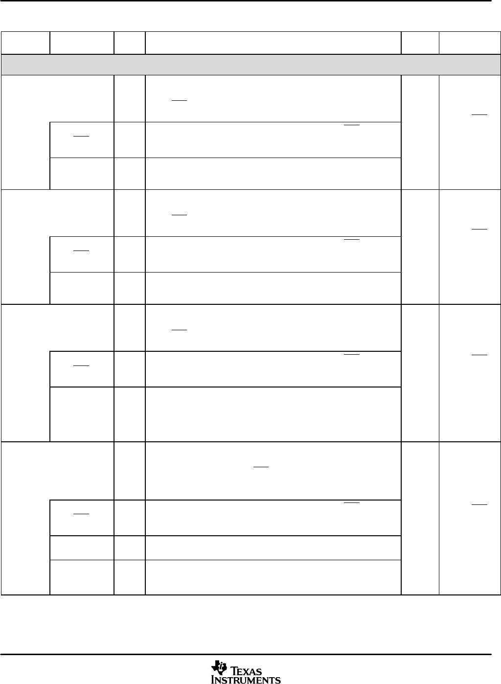
Table 2−3. Signal Descriptions (Continued)
TERMINAL
NAME
RESET
CONDITION
BK
‡
FUNCTIONI/O/Z
†
MULTIPLEXED
SIGNAL NAME
PARALLEL BUS (CONTINUED)
C4 I/O/Z
EMIF chip select for memory space CE0 or general-purpose IO9. This pin
serves in one of two functions: EMIF chip select for memory space CE0
(EMIF.CE0) or general-purpose IO9 (GPIO9). The initial state of this pin
depends on the GPIO0 pin. See Section 3.5.1 for more information.
GPIO0 = 1:
Output,
EMIF.CE0 O/Z
Active-low EMIF chip select for memory space CE0. EMIF.CE0 is selected
when the Parallel Port Mode bit field of the External Bus Selection Register
is set to 00 or 01.
BK
GPIO0 = 0:
Input,
GPIO9 I/O/Z
General-purpose IO9. GPIO9 is selected when the Parallel Port Mode bit
field of the External Bus Selection Register is set to 10 or 11.
GPIO9
C5 I/O/Z
EMIF chip select for memory space CE1 or general-purpose IO10. This pin
serves in one of two functions: EMIF chip-select for memory space CE1
(EMIF.CE1) or general-purpose IO10 (GPIO10). The initial state of this pin
depends on the GPIO0 pin. See Section 3.5.1 for more information.
GPIO0 = 1:
Output,
EMIF.CE1 O/Z
Active-low EMIF chip select for memory space CE1. EMIF.CE1 is selected
when the Parallel Port Mode bit field of the External Bus Selection Register
is set to 00 or 01.
BK
GPIO0 = 0:
Input,
GPIO10 I/O/Z
General-purpose IO10. GPIO10 is selected when the Parallel Port Mode
bit field of the External Bus Selection Register is set to 10 or 11.
GPIO10
C6 I/O/Z
EMIF chip select for memory space CE2 or HPI control input 0. This pin
serves in one of two functions: EMIF chip-select for memory space CE2
(EMIF.CE2) or HPI control input 0 (HPI.HCNTL0). The initial state of this
pin depends on the GPIO0 pin. See Section 3.5.1 for more information.
GPIO0 = 1:
EMIF.CE2 O/Z
Active-low EMIF chip select for memory space CE2. EMIF.CE2 is selected
when the Parallel Port Mode bit field of the External Bus Selection Register
is set to 00 or 01.
BK
EMIF.CE2
GPIO0 = 0:
HPI.HCNTL0 I
HPI control input 0. This pin, in conjunction with HPI.HCNTL1, selects a
host access to one of the three HPI registers. HPI.HCNTL0 is selected
when the Parallel Port Mode bit field of the External Bus Selection Register
is set to 10 or 11.
Input,
HPI.HCNTL0
C7 I/O/Z
EMIF chip select for memory space CE3, general-purpose IO11, or HPI
control input 1. This pin serves in one of three functions: EMIF chip-select
for memory space CE3 (EMIF.CE3), general-purpose IO11 (GPIO11), or
HPI control input 1 (HPI.HCNTL1). The initial state of this pin depends on
the GPIO0 pin. See Section 3.5.1 for more information.
GPIO0 = 1:
EMIF.CE3 O/Z
Active-low EMIF chip select for memory space CE3. EMIF.CE3 is selected
when the Parallel Port Mode bit field is of the External Bus Selection
Register set to 00 or 01.
BK
EMIF.CE3
GPIO0 = 0:
GPIO11 I/O/Z
General-purpose IO11. GPIO11 is selected when the Parallel Port Mode
bit field is set to 10.
Input,
HPI.HCNTL1
HPI.HCNTL1 I
HPI control input 1. This pin, in conjunction with HPI.HCNTL0, selects a
host access to one of the three HPI registers. The HPI.HCNTL1 mode is
selected when the Parallel Port Mode bit field is set to 11.
†
I = Input, O = Output, S = Supply, Hi-Z = High-impedance
‡
BK = bus keeper (the bus keeper maintains the previous voltage level during reset or while the output pin is not driven), PU = pullup,
PD = pulldown, H = hysteresis input buffer, FS = fail-safe buffer


