Electrical Specifications
136
November 2002 − Revised January 2005SPRS205D
5.19 Universal Serial Bus (USB) Timings
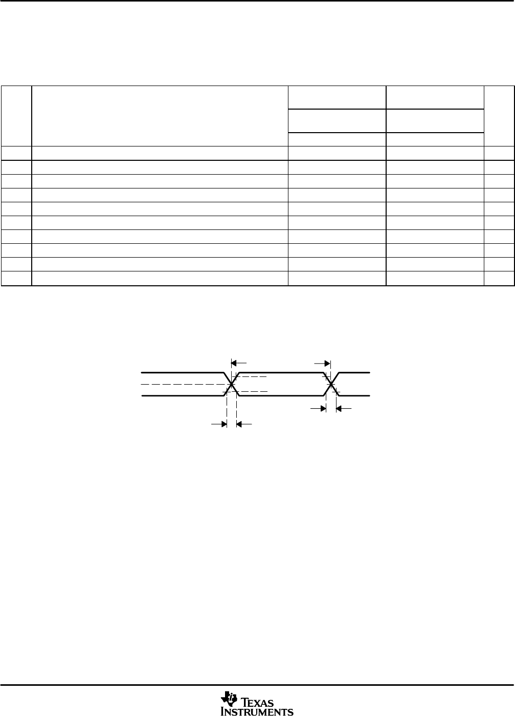
Table 5−45 assumes testing over recommended operating conditions (see Figure 5−41 and Figure 5−42).
Table 5−45. Universal Serial Bus (USB) Characteristics
CV
DD
= 1.2 V
CV
DD
= 1.35 V
CV
DD
= 1.6 V
NO. PARAMETER
FULL SPEED
12Mbps
FULL SPEED
12Mbps
UNIT
MIN TYP MAX MIN TYP MAX
U1 t
r
Rise time of DP and DN signals
†
4 20 4 20 ns
U2 t
f
Fall time of DP and DN signals
†
4 20 4 20 ns
t
RFM
Rise/Fall time matching
‡
90 111.11 90 111.11 %
V
CRS
Output signal cross-over voltage
†
1.3 2.0 1.3 2.0 V
t
jr
Differential propagation jitter
§¶
−2 2 −2 2 ns
f
op
Operating frequency (Full speed mode) 12 12 Mb/s
U3 R
s(DP)
Series resistor 24 24 Ω
U4 R
s(DN)
Series resistor 24 24 Ω
U5 C
edge(DP)
Edge rate control capacitor 22 22 pF
U6 C
edge(DN)
Edge rate control capacitor 22 22 pF
†
C
L
= 50 pF
‡
(t
r
/t
f
) x 100
§
t
px(1)
− t
px(0)
¶
USB PLL is susceptible to power supply ripple, refer to recommend operating conditions for allowable supply ripple to meet the USB peak-to-peak
jitter specification.
V
OL
U1
U2
V
CRS
V
OH
t
period
+ Jitter
90%
10%
D−
D+
Figure 5−41. USB Timings


