Electrical Specifications
131
November 2002 − Revised January 2005 SPRS205D
5.16 I
2
C Timings
Table 5−39 and Table 5−40 assume testing over recommended operating conditions (see Figure 5−37 and
Figure 5−38).
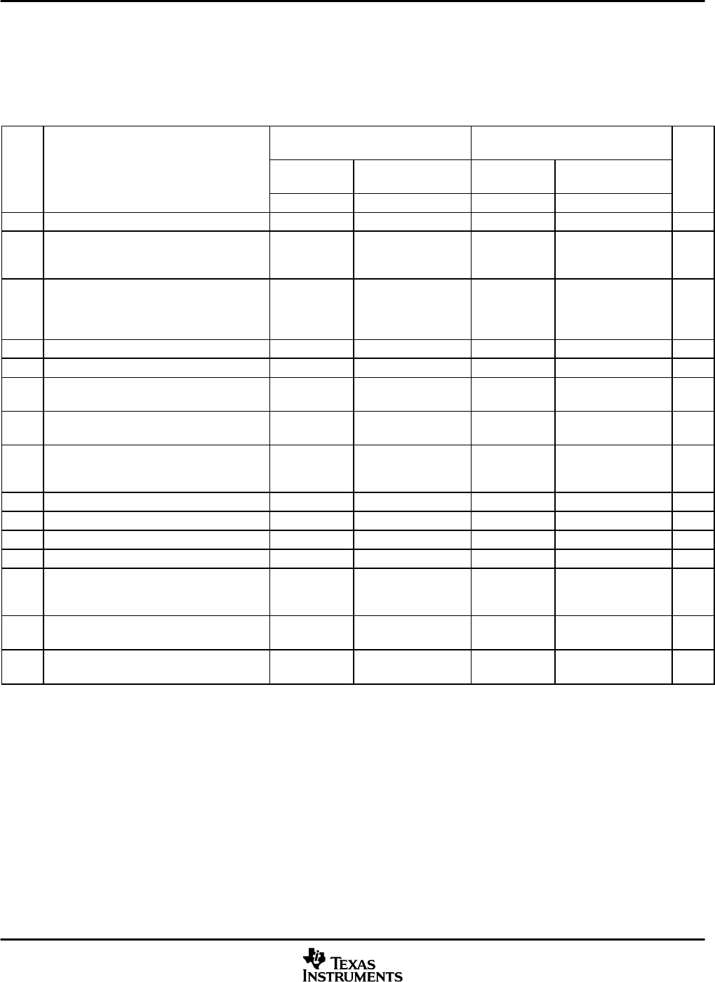
Table 5−39. I
2
C Signals (SDA and SCL) Timing Requirements
CV
DD
= 1.2 V
CV
DD
= 1.35 V
CV
DD
= 1.6 V
NO.
STANDARD
MODE
FAST
MODE
STANDARD
MODE
FAST
MODE
UNIT
MIN MAX MIN MAX MIN MAX MIN MAX
IC1 t
c(SCL)
Cycle time, SCL 10 2.5 10 2.5 µs
IC2 t
su(SCLH-SDAL)
Setup time, SCL high
before SDA low for a
repeated START condition
4.7 0.6 4.7 0.6 µs
IC3 t
h(SCLL-SDAL)
Hold time, SCL low after
SDA low for a START and
a repeated START
condition
4 0.6 4 0.6 µs
IC4 t
w(SCLL)
Pulse duration, SCL low 4.7 1.3 4.7 1.3 µs
IC5 t
w(SCLH)
Pulse duration, SCL high 4 0.6 4 0.6 µs
IC6 t
su(SDA-SCLH)
Setup time, SDA valid
before SCL high
250 100
†
250 100
†
ns
IC7 t
h(SDA-SCLL)
Hold time, SDA valid after
SCL low
0
‡
0
‡
0.9
§
0
‡
0
‡
0.9
§
µs
IC8 t
w(SDAH)
Pulse duration, SDA high
between STOP and
START conditions
4.7 1.3 4.7 1.3 µs
IC9 t
r(SDA)
Rise time, SDA 1000 20 + 0.1C
b
¶
300 1000 20 + 0.1C
b
¶
300 ns
IC10 t
r(SCL)
Rise time, SCL 1000 20 + 0.1C
b
¶
300 1000 20 + 0.1C
b
¶
300 ns
IC11 t
f(SDA)
Fall time, SDA 300 20 + 0.1C
b
¶
300 300 20 + 0.1C
b
¶
300 ns
IC12 t
f(SCL)
Fall time, SCL 300 20 + 0.1C
b
¶
300 300 20 + 0.1C
b
¶
300 ns
IC13 t
su(SCLH-SDAH)
Setup time, SCL high be-
fore SDA high (for STOP
condition)
4.0 0.6 4.0 0.6 µs
IC14 t
w(SP)
Pulse duration, spike
(must be suppressed)
0 50 0 50 ns
IC15 C
b
¶
Capacitive load for each
bus line
400 400 400 400 pF
†
A Fast-mode I
2
C-bus device can be used in a Standard-mode I
2
C-bus system, but the requirement t
su(SDA-SCLH)
≥ 250 ns must then be met.
This will automatically be the case if the device does not stretch the LOW period of the SCL signal. If such a device does stretch the LOW period
of the SCL signal, it must output the next data bit to the SDA line t
r
max + t
su(SDA-SCLH)
= 1000 + 250 = 1250 ns (according to the Standard-mode
I
2
C-Bus Specification) before the SCL line is released.
‡
A device must internally provide a hold time of at least 300 ns for the SDA signal (referred to the V
IHmin
of the SCL signal) to bridge the undefined
region of the falling edge of SCL.
§
The maximum t
h(SDA-SCLL)
has only to be met if the device does not stretch the LOW period [t
w(SCLL)
] of the SCL signal.
¶
C
b
= total capacitance of one bus line in pF. If mixed with HS-mode devices, faster fall-times are allowed.
I
2
C Bus is a trademark of Koninklijke Philips Electronics N.V.


