Freelance Electronics Components Distributor
Closed Dec 25th-26th
800-300-1968
We Stock Hard to Find Parts

TMS320VC5509APGE

Part # TMS320VC5509APGE
Description FIXED POINT DIGITAL SIGNAL PROCESSOR -DSP, 32 BIT, 200MHZ
Category IC
Availability Out of Stock
Qty 0
Qty Price
1 + $22.73692


Technical Document


DISCLAIMER: The information provided herein is solely for informational purposes. Customers must be aware of the suitability of this product for their application, and consider that variable factors such as Manufacturer, Product Category, Date Codes, Pictures and Descriptions may differ from available inventory.

Electrical Specifications
124
November 2002 − Revised January 2005SPRS205D
5.14.4 McBSP General-Purpose I/O Timings
Table 5−35 and Table 5−36 assume testing over recommended operating conditions (see Figure 5−30).
Table 5−35. McBSP General-Purpose I/O Timing Requirements
NO.
CV
DD
= 1.2 V
CV
DD
= 1.35 V
CV
DD
= 1.6 V
UNIT
NO.
MIN MAX MIN MAX
UNIT
MC20 t
su(MGPIO-COH)
Setup time, MGPIOx input mode before CLKOUT high
7 7 ns
MC21 t
h(COH-MGPIO)
Hold time, MGPIOx input mode after CLKOUT high
0 0 ns
MGPIOx refers to CLKRx, FSRx, DRx, CLKXx, or FSXx when configured as a general-purpose input.
Table 5−36. McBSP General-Purpose I/O Switching Characteristics
NO.
PARAMETER
CV
DD
= 1.2 V
CV
DD
= 1.35 V
CV
DD
= 1.6 V
UNIT
NO.
PARAMETER
MIN MAX MIN MAX
UNIT
MC22 t
d(COH-MGPIO)
Delay time, CLKOUT high to MGPIOx output mode
0 7 0 7 ns
MGPIOx refers to CLKRx, FSRx, CLKXx, FSXx, or DXx when configured as a general-purpose output.
CLKOUT
MGPIO
Input Mode
MGPIO
§
Output Mode
MC20
MC21
MC22
CLKOUT reflects the CPU clock.
MGPIOx refers to CLKRx, FSRx, DRx, CLKXx, or FSXx when configured as a general-purpose input.
§
MGPIOx refers to CLKRx, FSRx, CLKXx, FSXx, or DXx when configured as a general-purpose output.
Figure 5−30. McBSP General-Purpose I/O Timings
Electrical Specifications
125
November 2002 − Revised January 2005 SPRS205D
5.15 Enhanced Host-Port Interface (EHPI) Timings
Table 5−37 and Table 5−38 assume testing over recommended operating conditions (see Figure 5−31
through Figure 5−36).
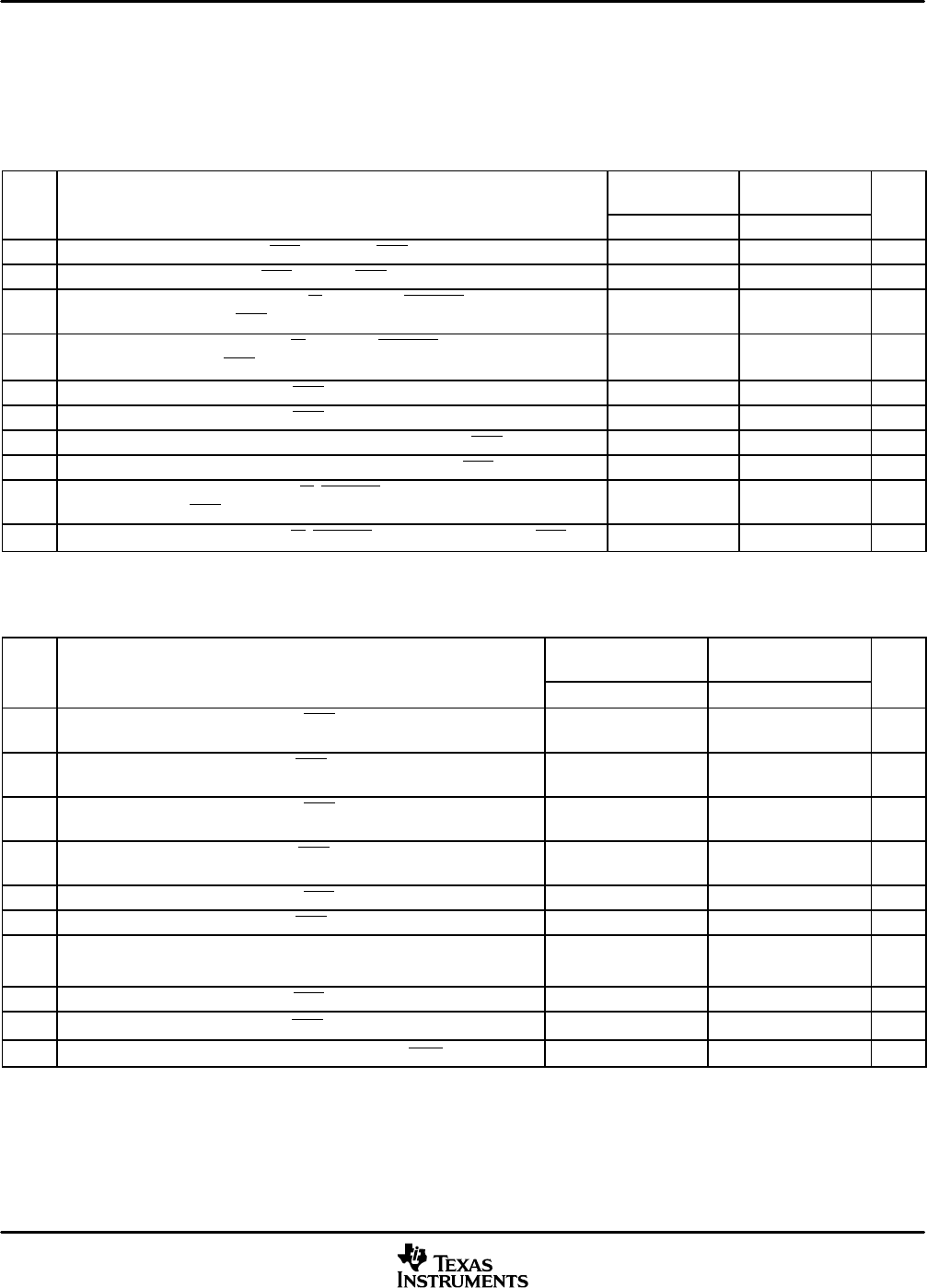
Table 5−37. EHPI Timing Requirements
NO.
CV
DD
= 1.2 V
CV
DD
= 1.35 V
CV
DD
= 1.6 V
UNIT
NO.
MIN MAX MIN MAX
UNIT
E11 t
su(HASL-HDSL)
Setup time, HAS low before HDS low 4 4 ns
E12 t
h(HDSL-HASL)
Hold time, HAS low after HDS low 3 3 ns
E13 t
su(HCNTLV-HDSL)
Setup time, (HR/W, HA[13:0], HBE[1:0], HCNTL[1:0]) valid
before HDS low
2 2 ns
E14 t
h(HDSL-HCNTLIV)
Hold time, (HR/W, HA[13:0], HBE[1:0], HCNTL[1:0]) invalid
after HDS low
4 4 ns
E15 t
w(HDSL)
Pulse duration, HDS low 4P
4P
ns
E16 t
w(HDSH)
Pulse duration, HDS high 4P
4P
ns
E17 t
su(HDV-HDSH)
Setup time, HD bus write data valid before HDS high 3 3 ns
E18 t
h(HDSH-HDIV)
Hold time, HD bus write data invalid after HDS high 4 4 ns
E19 t
su(HCNTLV-HASL)
Setup time, (HR/W, HBE[1:0], HCNTL[1:0]) valid before
HAS low
3 3 ns
E20 t
h(HASL-HCNTLIV)
Hold time, (HR/W, HBE[1:0], HCNTL[1:0]) valid after HAS low 4 4 ns
P = 1/CPU clock frequency in ns. For example, when running parts at 200 MHz, use P = 5 ns.
Table 5−38. EHPI Switching Characteristics
NO
.
PARAMETER
CV
DD
= 1.2 V
CV
DD
= 1.35 V
CV
DD
= 1.6 V
UNIT
NO.
PARAMETER
MIN MAX MIN MAX
UNIT
E1 t
en(HDSL-HDD)M
Enable time, HDS low to HD bus enabled
(memory access)
6 26 6 19 ns
E2 t
d(HDSL-HDV)M
Delay time, HDS low to HD bus read data valid
(memory access)
14P
†‡
14P
†‡
ns
E4 t
en(HDSL-HDD)R
Enable time, HDS low to HD enabled
(register access)
6 26 6 19 ns
E5 t
d(HDSL-HDV)R
Delay time, HDS low to HD bus read data valid
(register access)
26 19 ns
E6 t
dis(HDSH-HDIV)
Disable time, HDS high to HD bus read data invalid 6 26 6 19 ns
E7 t
d(HDSL-HRDYL)
Delay time, HDS low to HRDY low (during reads) 18 15 ns
E8
t
d(HDV-HRDYH)
Delay time, HD bus valid to HRDY high
(during reads)
2 2 ns
E9 t
d(HDSH-HRDYL)
Delay time, HDS high to HRDY low (during writes) 18 15 ns
E10
t
d(HDSH-HRDYH)
Delay time, HDS high to HRDY high (during writes) 14P
†‡
14P
†‡
ns
E21
t
d(COH-HINT)
Delay time, CLKOUT high to HINT high/low 0 11 0 8 ns
P = 1/CPU clock frequency in ns. For example, when running parts at 200 MHz, use P = 5 ns.
EHPI latency is dependent on the number of DMA channels active, their priorities and their source/destination ports. The latency shown assumes
no competing CPU or DMA activity to the memory resource being accessed by the EHPI.
Electrical Specifications
126
November 2002 − Revised January 2005SPRS205D
E21
CLKOUT
HINT
CLKOUT reflects the CPU clock.
Figure 5−31. HINT Timings
HCNTL0
HR/W
Read Data
Valid
HRDY
HA[13:0]
HDS
HCS
HD[15:0]
(read)
Valid
E16
E14
E13
E1
E10
E2
Valid Valid
Write Data
HD[15:0]
(write)
E15
E17 E18
Read Write
E6
E8E7 E9
E13
E14
E15
HBE[1:0]
Valid Valid
NOTES: A. Any non-multiplexed access with HCNTL0 low will result in HPIC register access. For data read or write, HCNTL0 must stay high
during the EHPI access.
B. The falling edge of HCS must occur concurrent with or before the falling edge of HDS. The rising edge of HCS must occur
concurrent with or after the rising edge of HDS. If HDS1 and/or HDS2 are tied permanently active and HCS is used as a strobe,
the timing requirements shown for HDS apply to HCS. HRDY is always driven to the same value as its internal state.
Figure 5−32. EHPI Nonmultiplexed Read/Write Timings
PREVIOUS3536373839404142434445464748NEXT