Electrical Specifications
122
November 2002 − Revised January 2005SPRS205D
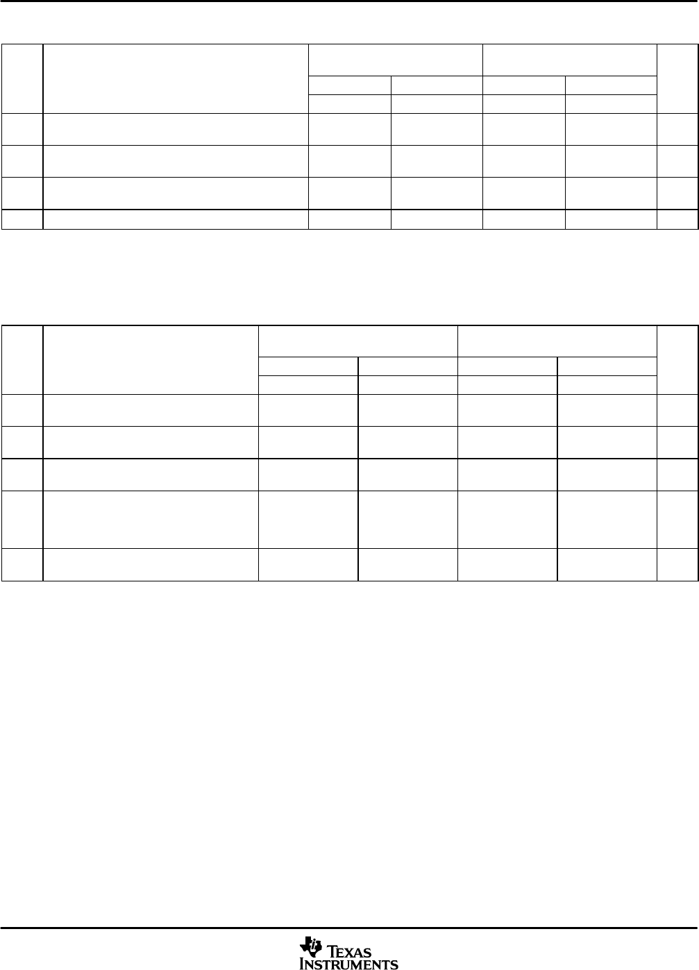
Table 5−33. McBSP as SPI Master or Slave Timing Requirements (CLKSTP = 11b, CLKXP = 1)
†
‡
CV
DD
= 1.2 V
CV
DD
= 1.35 V
CV
DD
= 1.6 V
NO.
MASTER SLAVE MASTER SLAVE
UNIT
MIN MAX MIN MAX MIN MAX MIN MAX
MC23 t
su(DRV-CKXL)
Setup time, DR valid before CLKX
low
15 3 − 6P 10 3 − 6P ns
MC24 t
h(CKXL-DRV)
Hold time, DR valid after CLKX
low
0 3 + 6P 0 3 + 6P ns
MC36 t
su(FXL-CKXL)
Setup time, FSX low before CLKX
low
5 5 ns
MC26 t
c(CKX)
Cycle time, CLKX 2P 16P 2P 16P ns
†
For all SPI slave modes, CLKG is programmed as 1/2 of the CPU clock by setting CLKSM = CLKGDV = 1.
‡
P = 1/CPU clock frequency. For example, when running parts at 200 MHz, use P = 5 ns. In addition to CPU frequency, the maximum operating
frequency of the serial port also depends on meeting the rest of the switching characteristics and timing requirements parameters specified.
Table 5−34. McBSP as SPI Master or Slave Switching Characteristics (CLKSTP = 11b, CLKXP = 1)
†
‡
CV
DD
= 1.2 V
CV
DD
= 1.35 V
CV
DD
= 1.6 V
NO. PARAMETER
MASTER
§
SLAVE MASTER
§
SLAVE
UNIT
MIN MAX MIN MAX MIN MAX MIN MAX
MC37 t
d(CKXH-FXL)
Delay time, CLKX high
to FSX low
¶
D − 5 D + 5 D − 4 D + 4 ns
MC38 t
d(FXL-CKXL)
Delay time, FSX low to
CLKX low
#
T − 5 T + 5 T − 4 T + 4 ns
MC29 t
d(CKXH-DXV)
Delay time, CLKX high
to DX valid
−4 6 3P + 3 5P + 15 −3 3 3P + 3 5P + 8 ns
MC39 t
dis(CKXH-DXHZ)
Disable time, DX high-
impedance following
last data bit from CLKX
high
−4 4 3P + 4 3P + 19 −3 1 3P + 3 3P + 12 ns
MC32 t
d(FXL-DXV)
Delay time, FSX low to
DX valid
C − 4 C + 4 3P + 4 3P + 18 C − 3 C + 3 3P + 4 3P + 10 ns
†
For all SPI slave modes, CLKG is programmed as 1/2 of the CPU clock by setting CLKSM = CLKGDV = 1.
‡
P = 1/CPU clock frequency. For example, when running parts at 200 MHz, use P = 5 ns. In addition to CPU frequency, the maximum operating
frequency of the serial port also depends on meeting the rest of the switching characteristics and timing requirements parameters specified.
§
T = CLKX period = (1 + CLKGDV) * P
C = CLKX low pulse width = T/2 when CLKGDV is odd or zero and = (CLKGDV/2) * P when CLKGDV is even
D = CLKX high pulse width = T/2 when CLKGDV is odd or zero and = (CLKGDV/2 + 1) * P when CLKGDV is even
¶
FSRP = FSXP = 1. As a SPI master, FSX is inverted to provide active-low slave-enable output. As a slave, the active-low signal input on FSX
and FSR is inverted before being used internally.
CLKXM = FSXM = 1, CLKRM = FSRM = 0 for master McBSP
CLKXM = CLKRM = FSXM = FSRM = 0 for slave McBSP
#
FSX should be low before the rising edge of clock to enable slave devices and then begin a SPI transfer at the rising edge of the master clock
(CLKX).


