Freelance Electronics Components Distributor
Closed Dec 25th-26th
800-300-1968
We Stock Hard to Find Parts

TMS320VC5509APGE

Part # TMS320VC5509APGE
Description FIXED POINT DIGITAL SIGNAL PROCESSOR -DSP, 32 BIT, 200MHZ
Category IC
Availability Out of Stock
Qty 0
Qty Price
1 + $22.73692


Technical Document


DISCLAIMER: The information provided herein is solely for informational purposes. Customers must be aware of the suitability of this product for their application, and consider that variable factors such as Manufacturer, Product Category, Date Codes, Pictures and Descriptions may differ from available inventory.

Electrical Specifications
112
November 2002 − Revised January 2005SPRS205D
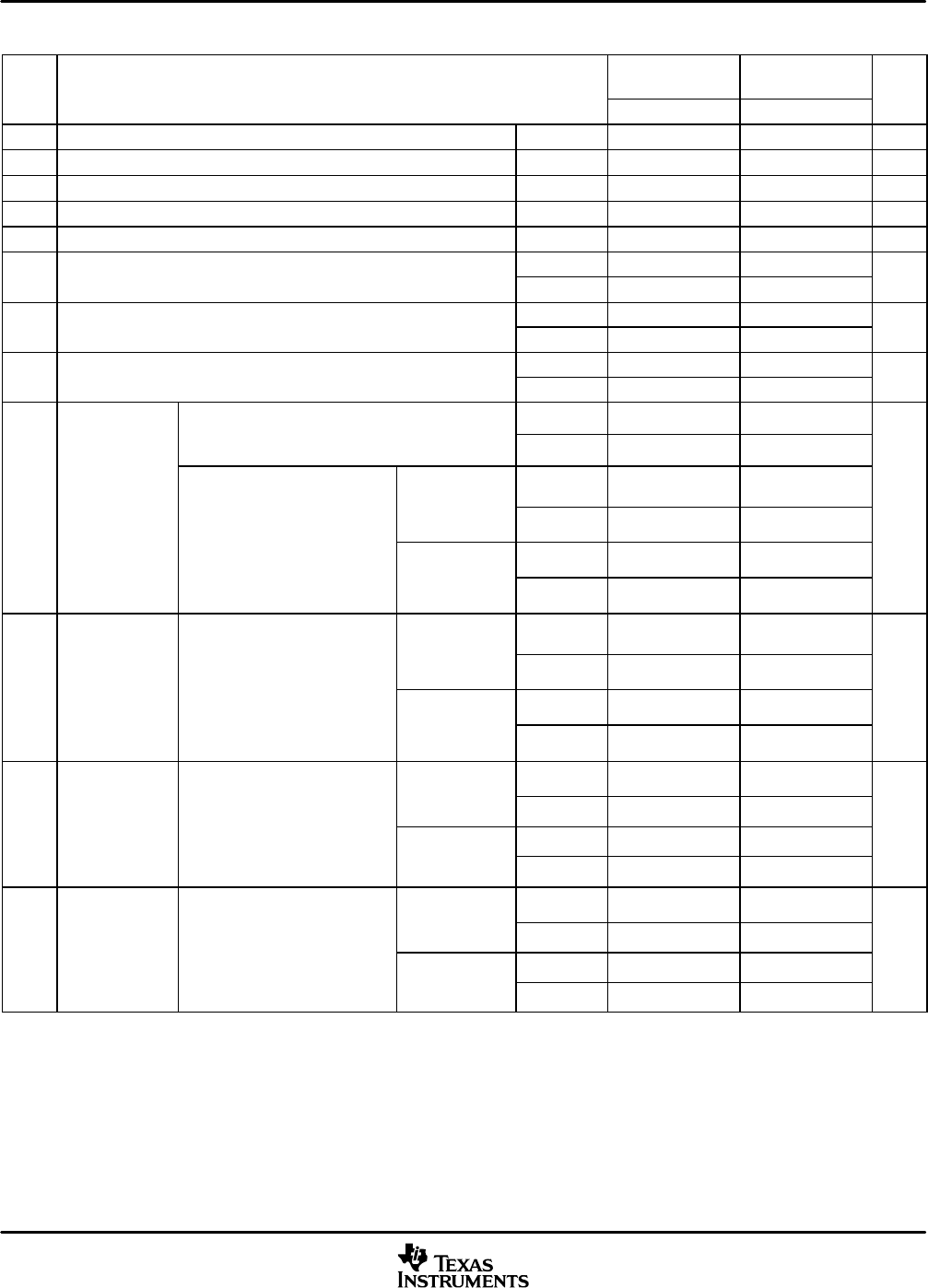
Table 5−24. McBSP0 Switching Characteristics
†‡
NO.
PARAMETER
CV
DD
= 1.2 V
CV
DD
= 1.35 V
CV
DD
= 1.6 V
UNIT
NO.
PARAMETER
MIN MAX MIN MAX
UNIT
MC1 t
c(CKRX)
Cycle time, CLKR/X CLKR/X int 2P 2P ns
MC3 t
r(CKRX)
Rise time, CLKR/X CLKR/X int 1 1 ns
MC4 t
f(CKRX)
Fall time, CLKR/X CLKR/X int 1 1 ns
MC11 t
w(CKRXH)
Pulse duration, CLKR/X high CLKR/X int D−2
§
D+2
§
D−1
§
D+1
§
ns
MC12 t
w(CKRXL)
Pulse duration, CLKR/X low CLKR/X int C−2
§
C+2
§
C−1
§
C+1
§
ns
MC13
t
d(CKRH-FRV)
Delay time, CLKR high to internal FSR valid
CLKR int −2 1 −2 1
ns
MC13
t
d(CKRH-FRV)
Delay time, CLKR high to internal FSR valid
CLKR ext 4 13 4 8
ns
MC14
t
d(CKXH-FXV)
Delay time, CLKX high to internal FSX valid
CLKX int −2 2 −2 2
ns
MC14
t
d(CKXH-FXV)
Delay time, CLKX high to internal FSX valid
CLKX ext 4 15 4 9
ns
MC15
t
dis(CKXH-DXHZ)
Disable time, DX high-impedance from CLKX high
CLKX int 0 5 −5 1
ns
MC15
t
dis(CKXH-DXHZ)
Disable time, DX high-impedance from CLKX high
following last data bit
CLKX ext 10 18 3 11
ns
Delay time, CLKX high to DX valid.
This applies to all bits except the first bit
CLKX int 5 4
This applies to all bits except the first bit
transmitted.
CLKX ext 15 9
MC16
t
d(CKXH-DXV)
Delay time, CLKX high to DX
valid
DXENA = 0
CLKX int 4 2
ns
MC16
t
d(CKXH-DXV)
valid
Only applies to first bit
DXENA = 0
CLKX ext 13 7
ns
Only applies to first b
it
transmitted when in Data Dela
y
1 or 2 (XDATDLY = 01b or 10b)
DXENA = 1
CLKX int 2P + 1 2P + 1
transmitted when in Data Delay
1 or 2 (XDATDLY = 01b or 10b
)
modes
DXENA = 1
CLKX ext 2P + 4 2P + 3
Enable time, DX driven from
CLKX high
DXENA = 0
CLKX int −1 −3
MC17
t
en(CKXH-DX)
CLKX high
Only applies to first bit
DXENA = 0
CLKX ext 6 3
ns
MC17
t
en(CKXH-DX)
Only applies to first b
it
transmitted when in Data Dela
y
1 or 2 (XDATDLY= 01b or 10b)
DXENA = 1
CLKX int P − 1 P − 3
ns
transmitted when in Data Delay
1 or 2 (XDATDLY= 01b or 10b
)
modes
DXENA = 1
CLKX ext P + 6 P + 3
Delay time, FSX high to DX
valid
DXENA = 0
FSX int 2 2
MC18
t
d(FXH-DXV)
valid
DXENA = 0
FSX ext 13 8
ns
MC18
t
d(FXH-DXV)
Only applies to first b
it
transmitted when in Data Delay
DXENA = 1
FSX int 2P + 1 2P + 1
ns
transmitted when in Data Delay
0 (XDATDLY= 00b) mode.
DXENA = 1
FSX ext 2P + 10 2P + 10
Enable time, DX driven from
FSX high
DXENA = 0
FSX int 0 0
MC19
t
en(FXH-DX)
FSX high
DXENA = 0
FSX ext 8 3
ns
MC19
t
en(FXH-DX)
Only applies to first b
it
transmitted when in Data Delay
DXENA = 1
FSX int P − 3 P − 3
ns
transmitted when in Data Delay
0 (XDATDLY= 00b) mode
DXENA = 1
FSX ext P + 8 P + 4
Polarity bits CLKRP = CLKXP = FSRP = FSXP = 0. If the polarity of any of the signals is inverted, then the timing references of that signal are
also inverted.
P = 1/CPU clock frequency. For example, when running parts at 200 MHz, use P = 5 ns. In addition to CPU frequency, the maximum operating
frequency of the serial port also depends on meeting the rest of the switching characteristics and timing requirements parameters specified.
§
T=CLKRX period = (1 + CLKGDV) * P
C=CLKRX low pulse width = T/2 when CLKGDV is odd or zero and = (CLKGDV/2) * P when CLKGDV is even
D=CLKRX high pulse width = T/2 when CLKGDV is odd or zero and = (CLKGDV/2 + 1) * P when CLKGDV is even
See the TMS320C55x DSP Peripherals Overview Reference Guide (literature number SPRU317) for a description of the DX enable (DXENA)
and data delay features of the McBSP.
Electrical Specifications
113
November 2002 − Revised January 2005 SPRS205D
5.14.2 McBSP1 and McBSP2 Timings
Table 5−25 and Table 5−26 assume testing over recommended operating conditions (see Figure 5−24 and
Figure 5−25).
Table 5−25. McBSP1 and McBSP2 Timing Requirements
NO.
CV
DD
= 1.2 V
CV
DD
= 1.35 V
CV
DD
= 1.6 V
UNIT
NO.
MIN MAX MIN MAX
UNIT
MC1 t
c(CKRX)
Cycle time, CLKR/X CLKR/X ext 2P
2P
ns
MC2 t
w(CKRX)
Pulse duration, CLKR/X high or CLKR/X low CLKR/X ext P–1
P–1
ns
MC3 t
r(CKRX)
Rise time, CLKR/X CLKR/X ext 6 6 ns
MC4 t
f(CKRX)
Fall time, CLKR/X CLKR/X ext 6 6 ns
MC5
t
su(FRH-CKRL)
Setup time, external FSR high before CLKR low
CLKR int 11 7
ns
MC5
t
su(FRH-CKRL)
Setup time, external FSR high before CLKR low
CLKR ext 3 3
ns
MC6
t
h(CKRL-FRH)
Hold time, external FSR high after CLKR low
CLKR int −3 −3
ns
MC6
t
h(CKRL-FRH)
Hold time, external FSR high after CLKR low
CLKR ext 1 1
ns
MC7
t
su(DRV-CKRL)
Setup time, DR valid before CLKR low
CLKR int 11 7
ns
MC7
t
su(DRV-CKRL)
Setup time, DR valid before CLKR low
CLKR ext 3 3
ns
MC8
t
h(CKRL-DRV)
Hold time, DR valid after CLKR low
CLKR int −2 −2
ns
MC8
t
h(CKRL-DRV)
Hold time, DR valid after CLKR low
CLKR ext 3 3
ns
MC9
t
su(FXH-CKXL)
Setup time, external FSX high before CLKX low
CLKX int 14 9
ns
MC9
t
su(FXH-CKXL)
Setup time, external FSX high before CLKX low
CLKX ext 4 3
ns
MC10
t
h(CKXL-FXH)
Hold time, external FSX high after CLKX low
CLKX int −3 −3
ns
MC10
t
h(CKXL-FXH)
Hold time, external FSX high after CLKX low
CLKX ext 1 1
ns
Polarity bits CLKRP = CLKXP = FSRP = FSXP = 0. If the polarity of any of the signals is inverted, then the timing references of that signal are
also inverted.
P = 1/CPU clock frequency. For example, when running parts at 200 MHz, use P = 5 ns. In addition to CPU frequency, the maximum operating
frequency of the serial port also depends on meeting the rest of the switching characteristics and timing requirements parameters specified.
Electrical Specifications
114
November 2002 − Revised January 2005SPRS205D
Table 5−26. McBSP1 and McBSP2 Switching Characteristics
†‡
NO.
PARAMETER
CV
DD
= 1.2 V
CV
DD
= 1.35 V
CV
DD
= 1.6 V
UNIT
NO.
PARAMETER
MIN MAX MIN MAX
UNIT
MC1 t
c(CKRX)
Cycle time, CLKR/X CLKR/X int 2P 2P ns
MC3 t
r(CKRX)
Rise time, CLKR/X CLKR/X int 2 2 ns
MC4 t
f(CKRX)
Fall time, CLKR/X CLKR/X int 2 2 ns
MC11 t
w(CKRXH)
Pulse duration, CLKR/X high CLKR/X int D − 2
§
D + 2
§
D − 2
§
D + 2
§
ns
MC12 t
w(CKRXL)
Pulse duration, CLKR/X low CLKR/X int C − 2
§
C + 2
§
C − 2
§
C + 2
§
ns
MC13
t
d(CKRH-FRV)
Delay time, CLKR high to internal FSR valid
CLKR int −3 2 −3 2
ns
MC13
t
d(CKRH-FRV)
Delay time, CLKR high to internal FSR valid
CLKR ext 3 14 3 9
ns
MC14
t
d(CKXH-FXV)
Delay time, CLKX high to internal FSX valid
CLKX int −3 2 −3 2
ns
MC14
t
d(CKXH-FXV)
Delay time, CLKX high to internal FSX valid
CLKX ext 4 15 4 9
ns
MC15
t
dis(CKXH-DXHZ)
Disable time, DX high-impedance from CLKX high
CLKX int −3 3 −5 1
ns
MC15
t
dis(CKXH-DXHZ)
Disable time, DX high-impedance from CLKX high
following last data bit
CLKX ext 10 19 3 12
ns
Delay time, CLKX high to DX valid.
This applies to all bits except the first bit
CLKX int 5 3
This applies to all bits except the first bit
transmitted.
CLKX ext 15 9
MC16
t
d(CKXH-DXV)
Delay time, CLKX high to DX
valid
DXENA = 0
CLKX int 4 2
ns
MC16
t
d(CKXH-DXV)
valid
Only applies to first bit
DXENA = 0
CLKX ext 15 9
ns
Only applies to first b
it
transmitted when in Data Dela
y
1 or 2 (XDATDLY=
DXENA = 1
CLKX int 2P + 1 2P + 1
transmitted when in Data Delay
1 or 2 (XDATDLY=
01b or 10b) modes
DXENA = 1
CLKX ext 2P + 5 2P + 3
Enable time, DX driven from
CLKX high
DXENA = 0
CLKX int −2 −4
MC17
t
en(CKXH-DX)
CLKX high
Only applies to first bit
DXENA = 0
CLKX ext 9 4
ns
MC17
t
en(CKXH-DX)
Only applies to first b
it
transmitted when in Data Dela
y
1 or 2 (XDATDLY=
DXENA = 1
CLKX int P − 2 P − 4
ns
transmitted when in Data Delay
1 or 2 (XDATDLY=
01b or 10b) modes
DXENA = 1
CLKX ext P + 9 P + 4
Delay time, FSX high to DX
valid
DXENA = 0
FSX int 3 2
MC18
t
d(FXH-DXV)
valid
DXENA = 0
FSX ext 13 8
ns
MC18
t
d(FXH-DXV)
Only applies to first b
it
transmitted when in Data Delay
DXENA = 1
FSX int 2P + 1 2P + 1
ns
transmitted when in Data Delay
0 (XDATDLY=00b) mode.
DXENA = 1
FSX ext 2P + 12 2P + 7
Enable time, DX driven from
FSX high
DXENA = 0
FSX int 1 0
MC19
t
en(FXH-DX)
FSX high
DXENA = 0
FSX ext 8 4
ns
MC19
t
en(FXH-DX)
Only applies to first b
it
transmitted when in Data Delay
DXENA = 1
FSX int P − 1 P − 3
ns
transmitted when in Data Delay
0 (XDATDLY=00b) mode
DXENA = 1
FSX ext P + 8 P + 5
Polarity bits CLKRP = CLKXP = FSRP = FSXP = 0. If the polarity of any of the signals is inverted, then the timing references of that signal are
also inverted.
P = 1/CPU clock frequency. For example, when running parts at 200 MHz, use P = 5 ns. In addition to CPU frequency, the maximum operating
frequency of the serial port also depends on meeting the rest of the switching characteristics and timing requirements parameters specified.
§
T=CLKRX period = (1 + CLKGDV) * P
C=CLKRX low pulse width = T/2 when CLKGDV is odd or zero and = (CLKGDV/2) * P when CLKGDV is even
D=CLKRX high pulse width = T/2 when CLKGDV is odd or zero and = (CLKGDV/2 + 1) * P when CLKGDV is even
See the TMS320C55x DSP Peripherals Overview Reference Guide (literature number SPRU317) for a description of the DX enable (DXENA)
and data delay features of the McBSP.
PREVIOUS3132333435363738394041424344NEXT