Freelance Electronics Components Distributor
Closed Dec 25th-26th
800-300-1968
We Stock Hard to Find Parts

TMS320VC5509APGE

Part # TMS320VC5509APGE
Description FIXED POINT DIGITAL SIGNAL PROCESSOR -DSP, 32 BIT, 200MHZ
Category IC
Availability Out of Stock
Qty 0
Qty Price
1 + $22.73692


Technical Document


DISCLAIMER: The information provided herein is solely for informational purposes. Customers must be aware of the suitability of this product for their application, and consider that variable factors such as Manufacturer, Product Category, Date Codes, Pictures and Descriptions may differ from available inventory.

Electrical Specifications
109
November 2002 − Revised January 2005 SPRS205D
5.12 General-Purpose Input/Output (GPIOx) Timings
Table 5−19 and Table 5−20 assume testing over recommended operating conditions (see Figure 5−21).
Table 5−19. GPIO Pins Configured as Inputs Timing Requirements
NO.
CV
DD
= 1.2 V
CV
DD
= 1.35 V
CV
DD
= 1.6 V
UNIT
NO.
MIN MAX MIN MAX
UNIT
Setup time, IOx input valid before CLKOUT
GPIO 4 4
G1 t
su(GPIO-COH)
Setup time, IOx input valid before CLKOUT
high
AGPIO
8 8
ns
G1
t
su(GPIO-COH)
high
EHPIGPIO
8 8
ns
Hold time, IOx input valid after CLKOUT
GPIO 0 0
G2 t
h(COH-GPIO)
Hold time, IOx input valid after CLKOUT
high
AGPIO
0 0 ns
h(COH-GPIO)
high
EHPIGPIO
0 0
AGPIO pins: A[15:0]
EHPIGPIO pins: C13, C10, C7, C5, C4, and C0
Table 5−20. GPIO Pins Configured as Outputs Switching Characteristics
NO.
PARAMETER
CV
DD
= 1.2 V
CV
DD
= 1.35 V
CV
DD
= 1.6 V
UNIT
NO.
PARAMETER
MIN MAX MIN MAX
UNIT
Delay time, CLKOUT high to IOx output
GPIO 0 6 0 6
G3 t
d(COH-GPIO)
Delay time, CLKOUT high to IOx outpu
t
change
AGPIO
0 11 0 11 ns
d(COH-GPIO)
change
EHPIGPIO
0 13 0 13
AGPIO pins: A[15:0]
EHPIGPIO pins: C13, C10, C7, C5, C4, and C0
G3
G1
G2
CLKOUT
IOx
Input Mode
IOx
Output Mode
CLKOUT reflects the CPU clock.
Figure 5−21. General-Purpose Input/Output (IOx) Signal Timings
Electrical Specifications
110
November 2002 − Revised January 2005SPRS205D
5.13 TIN/TOUT Timings (Timer0 Only)
Table 5−21 and Table 5−22 assume testing over recommended operating conditions (see Figure 5−22 and
Figure 5−23).
Table 5−21. TIN/TOUT Pins Configured as Inputs Timing Requirements
†‡
NO.
CV
DD
= 1.2 V
CV
DD
= 1.35 V
CV
DD
= 1.6 V
UNIT
NO.
MIN MAX MIN MAX
UNIT
T4 t
w(TIN/TOUTL)
Pulse width, TIN/TOUT low 2P + 1 2P + 1 ns
T5 t
w(TIN/TOUTH)
Pulse width, TIN/TOUT high 2P + 1 2P + 1 ns
P = 1/CPU clock frequency. For example, when running parts at 200 MHz, use P = 5 ns.
Only the Timer0 signal is externally available. The Timer1 signal is internally terminated and is not available for external use.
Table 5−22. TIN/TOUT Pins Configured as Outputs Switching Characteristics
†‡§
NO.
PARAMETER
CV
DD
= 1.2 V
CV
DD
= 1.35 V
CV
DD
= 1.6 V
UNIT
NO.
PARAMETER
MIN MAX MIN MAX
UNIT
T1 t
d(COH-TIN/TOUTH)
Delay time, CLKOUT high to TIN/TOUT high −1 3 −1 3 ns
T2 t
d(COH-TIN/TOUTL)
Delay time, CLKOUT high to TIN/TOUT low −1 3 −1 3 ns
T3 t
w(TIN/TOUT)
Pulse duration, TIN/TOUT (output) P − 1 P − 1 ns
P = 1/CPU clock frequency. For example, when running parts at 200 MHz, use P = 5 ns.
Only the Timer0 signal is externally available. The Timer1 signal is internally terminated and is not available for external use.
§
For proper operation of the TIN/TOUT pin configured as an output, the timer period must be configured for at least 4 cycles.
TIN/TOUT
as Input
T5
T4
Figure 5−22. TIN/TOUT Timings When Configured as Inputs
TIN/TOUT
as Output
CLKOUT
T2
T1
T3
Figure 5−23. TIN/TOUT Timings When Configured as Outputs
Electrical Specifications
111
November 2002 − Revised January 2005 SPRS205D
5.14 Multichannel Buffered Serial Port (McBSP) Timings
5.14.1 McBSP0 Timings
Table 5−23 and Table 5−24 assume testing over recommended operating conditions (see Figure 5−24 and
Figure 5−25).
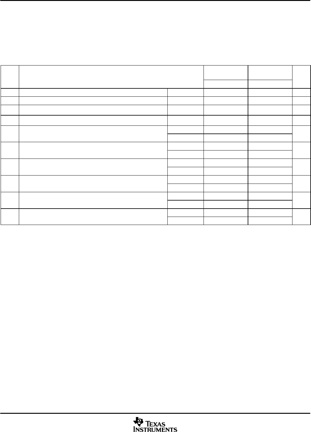
Table 5−23. McBSP0 Timing Requirements
NO.
CV
DD
= 1.2 V
CV
DD
= 1.35 V
CV
DD
= 1.6 V
UNIT
NO.
MIN MAX MIN MAX
UNIT
MC1 t
c(CKRX)
Cycle time, CLKR/X CLKR/X ext 2P
2P
ns
MC2 t
w(CKRX)
Pulse duration, CLKR/X high or CLKR/X low CLKR/X ext P–1
P–1
ns
MC3 t
r(CKRX)
Rise time, CLKR/X CLKR/X ext 6 6 ns
MC4 t
f(CKRX)
Fall time, CLKR/X CLKR/X ext 6 6 ns
MC5
t
su(FRH-CKRL)
Setup time, external FSR high before CLKR low
CLKR int 10 7
ns
MC5
t
su(FRH-CKRL)
Setup time, external FSR high before CLKR low
CLKR ext 2 2
ns
MC6
t
h(CKRL-FRH)
Hold time, external FSR high after CLKR low
CLKR int −3 −3
ns
MC6
t
h(CKRL-FRH)
Hold time, external FSR high after CLKR low
CLKR ext 1 1
ns
MC7
t
su(DRV-CKRL)
Setup time, DR valid before CLKR low
CLKR int 10 7
ns
MC7
t
su(DRV-CKRL)
Setup time, DR valid before CLKR low
CLKR ext 2 2
ns
MC8
t
h(CKRL-DRV)
Hold time, DR valid after CLKR low
CLKR int −2 −2
ns
MC8
t
h(CKRL-DRV)
Hold time, DR valid after CLKR low
CLKR ext 3 3
ns
MC9
t
su(FXH-CKXL)
Setup time, external FSX high before CLKX low
CLKX int 13 8
ns
MC9
t
su(FXH-CKXL)
Setup time, external FSX high before CLKX low
CLKX ext 3 2
ns
MC10
t
h(CKXL-FXH)
Hold time, external FSX high after CLKX low
CLKX int −3 −3
ns
MC10
t
h(CKXL-FXH)
Hold time, external FSX high after CLKX low
CLKX ext 1 1
ns
Polarity bits CLKRP = CLKXP = FSRP = FSXP = 0. If the polarity of any of the signals is inverted, then the timing references of that signal are
also inverted.
P = 1/CPU clock frequency. For example, when running parts at 200 MHz, use P = 5 ns. In addition to CPU frequency, the maximum operating
frequency of the serial port also depends on meeting the rest of the switching characteristics and timing requirements parameters specified.
PREVIOUS3031323334353637383940414243NEXT