Electrical Specifications
106
November 2002 − Revised January 2005SPRS205D
5.8.3 Warm Reset
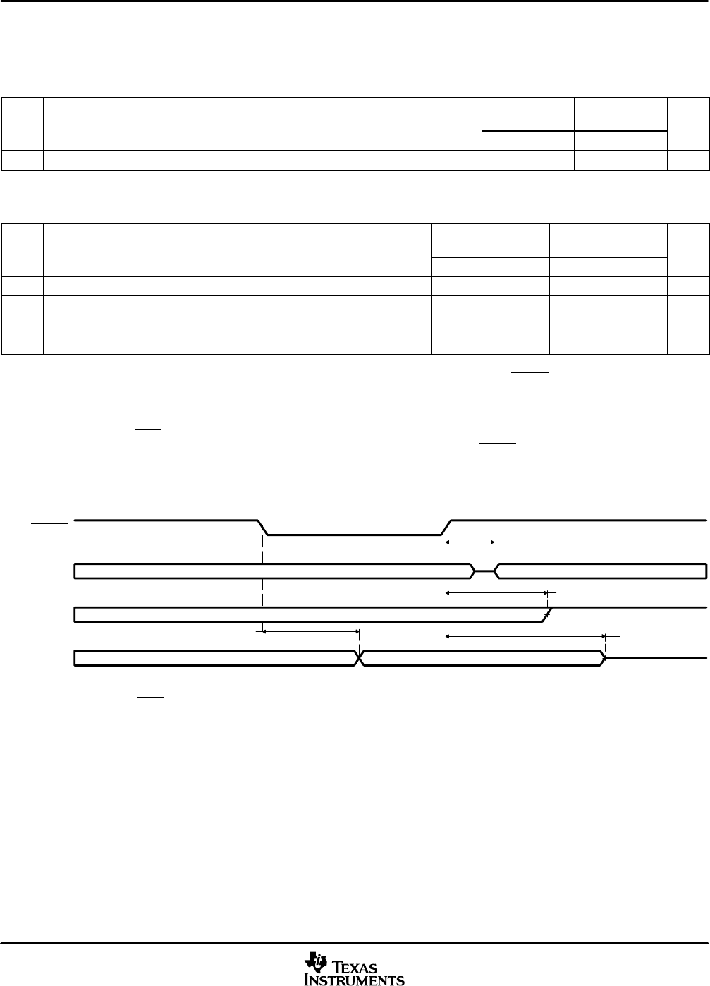
Table 5−14 and Table 5−15 assume testing over recommended operating conditions (see Figure 5−17).
Table 5−14. Reset Timing Requirements
CV
DD
= 1.2 V
CV
DD
= 1.35 V
CV
DD
= 1.6 V
MIN MAX MIN MAX
R4 t
w(RSL)
Pulse width, reset low 3P
†
3P
†
ns
†
P = 1/CPU clock frequency in ns. For example, when running parts at 200 MHz, use P = 5 ns.
Table 5−15. Reset Switching Characteristics
†
CV
DD
= 1.2 V
CV
DD
= 1.35 V
CV
DD
= 1.6 V
MIN MAX MIN MAX
R5 t
d(RSTH-BKV)
Delay time, reset high to BK group valid
‡
38P + 15 38P + 15 ns
R6 t
d(RSTH-HIGHV)
Delay time, reset high to High group valid
§
38P + 15 38P + 15 ns
R7 t
d(RSTL-ZIV)
Delay time, reset low to Z group invalid
¶
1P + 15 1P + 15 ns
R8 t
d(RSTH-ZV)
Delay time, reset high to Z group valid
¶
38P + 15 38P + 15 ns
†
P = 1/CPU clock frequency in ns. For example, when CPU is running at 200 MHz, P = 5 ns.
‡
BK group: Pins with bus keepers, holds previous state during reset. Following low-to-high transition of RESET, these pins go to their post-reset
logic state.
BK group pins: A’[0], A[15:0], D[15:0], C[14:2], C0, GPIO5, S13, and S23
§
High group: Following low-to-high transition of RESET, these pins go to logic-high state.
High group pins: C1[HPI.HINT], XF
¶
Z group: Bidirectional pins which become input or output pins. Following low-to-high transition of RESET, these pins go to high-impedance state.
Z group pins: C1[EMIF.AOE], GPIO[7:6, 4:0], TIN/TOUT0, SDA, SCL, CLKR0, FSRX0, CLKX0, DX0, FSX0, S[25:24, 22:20, 15:14, 12:10],
A[20:16]
RESET
BK Group
†
igh Group
‡
Z Group
§
R5
R7
R6
R8
†
BK group pins: A’[0], A[15:0], D[15:0], C[14:2], C0, GPIO5, S13, and S23
‡
High group pins: C1[HPI.HINT], XF
§
Z group pins: C1[EMIF.AOE], GPIO[7:6, 4:0], TIN/TOUT0, SDA, SCL, CLKR0, FSRX0, CLKX0, DX0, FSX0, S[25:24, 22:20, 15:14, 12:10]
A[20:16]
Figure 5−17. Reset Timings


