Electrical Specifications
104
November 2002 − Revised January 2005SPRS205D
5.8 Reset Timings
5.8.1 Power-Up Reset (On-Chip Oscillator Active)
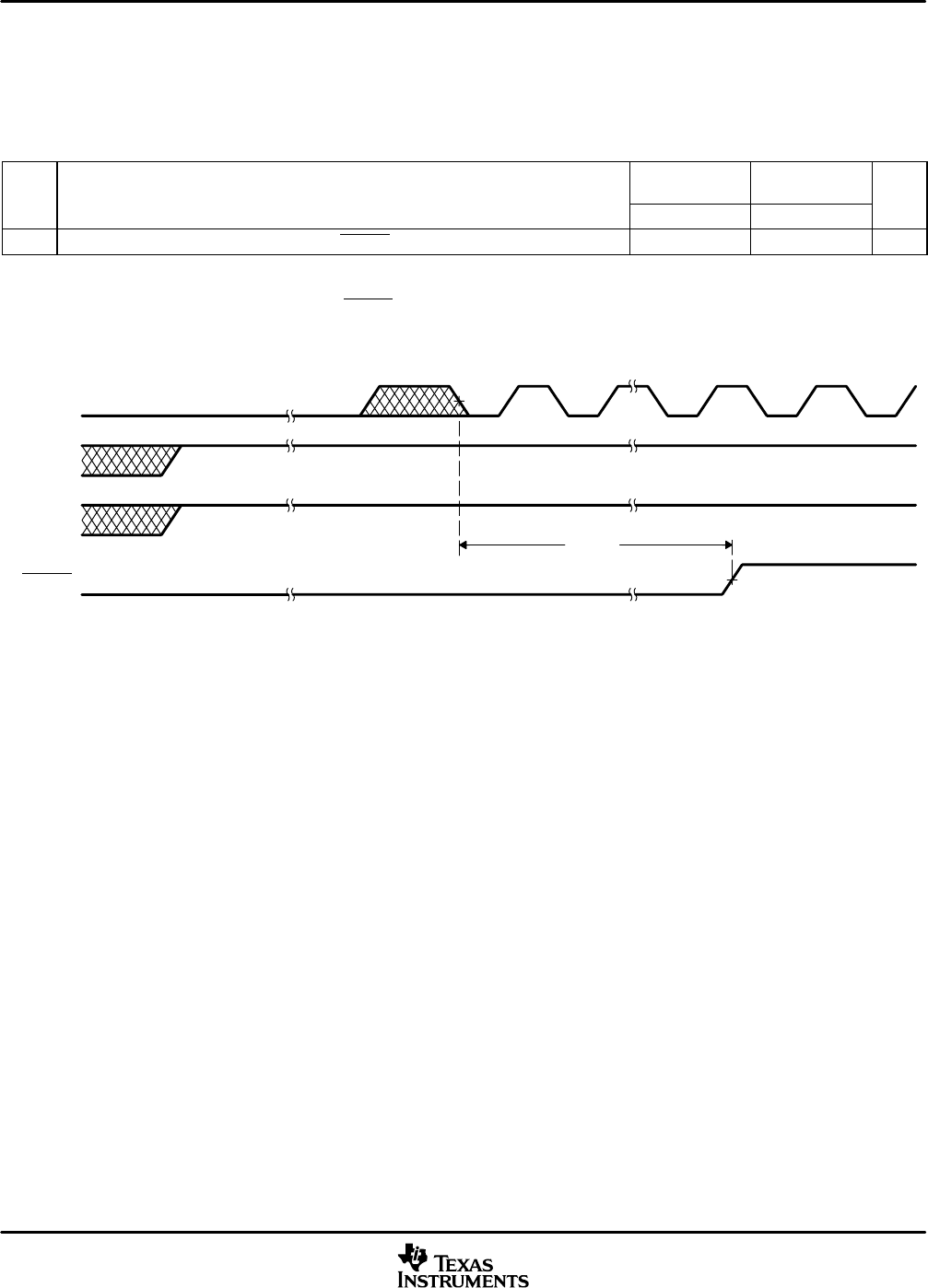
Table 5−11 assumes testing over recommended operating conditions (see Figure 5−15).
Table 5−11. Power-Up Reset (On-Chip Oscillator Active) Timing Requirements
CV
DD
= 1.2 V
CV
DD
= 1.35 V
CV
DD
= 1.6 V
MIN MAX MIN MAX
R1 t
h(SUPSTBL-RSTL)
Hold time, RESET low after oscillator stable
†
3P
‡
3P
‡
ns
†
Oscillator stable time depends on the crystal characteristic (i.e., frequency, ESR, etc.) which varies from one crystal manufacturer to another.
Based on the crystal characteristics, the oscillator stable time can be in the range of a few to 10s of ms. A reset circuit with 100 ms or more delay
time will ensure the oscillator stabilized before the RESET goes high.
‡
P = 1/(input clock frequency) in ns. For example, when input clock is 12 MHz, P = 83.33 ns.
R1
CLKOUT
CV
DD
DV
DD
RESET
Figure 5−15. Power-Up Reset (On-Chip Oscillator Active) Timings


