Electrical Specifications
96
November 2002 − Revised January 2005SPRS205D
5.7.2 Synchronous DRAM (SDRAM) Timings
Table 5−9 and Table 5−10 assume testing over recommended operating conditions (see Figure 5−8 through
Figure 5−14).
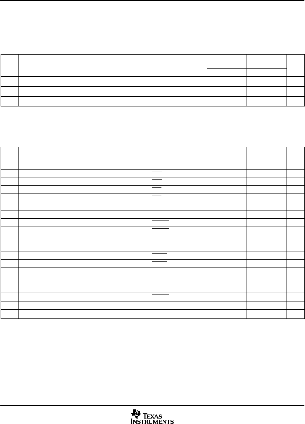
Table 5−9. Synchronous DRAM Cycle Timing Requirements
CV
DD
= 1.2 V
CV
DD
= 1.35 V
CV
DD
= 1.6 V
MIN MAX MIN MAX
M19 t
su(DV-CLKMEMH)
Setup time, read data valid before CLKMEM high 3 3 ns
M20 t
h(CLKMEMH-DV)
Hold time, read data valid after CLKMEM high 2 2 ns
M21 t
c(CLKMEM)
Cycle time, CLKMEM 9.26
†
7.52
‡
ns
†
Maximum SDRAM operating frequency = 108 MHz. Actual attainable maximum operating frequency will depend on the quality of the PC board
design and the memory chip timing requirement.
‡
Maximum SDRAM operating frequency = 133 MHz. Actual attainable maximum operating frequency will depend on the quality of the PC board
design and the memory chip timing requirement.
Table 5−10. Synchronous DRAM Cycle Switching Characteristics
CV
DD
= 1.2 V
CV
DD
= 1.35 V
CV
DD
= 1.6 V
MIN MAX MIN MAX
M22 t
d(CLKMEMH-CEL)
Delay time, CLKMEM high to CEx low 1.2 7 1.2 5 ns
M23 t
d(CLKMEMH-CEH)
Delay time, CLKMEM high to CEx high 1.2 7 1.2 5 ns
M24 t
d(CLKMEMH-BEV)
Delay time, CLKMEM high to BEx valid 1.2 7 1.2 5 ns
M25 t
d(CLKMEMH-BEIV)
Delay time, CLKMEM high to BEx invalid 1.2 7 1.2 5 ns
M26 t
d(CLKMEMH-AV)
Delay time, CLKMEM high to address valid 1.2 7 1.2 5 ns
M27 t
d(CLKMEMH-AIV)
Delay time, CLKMEM high to address invalid 1.2 7 1.2 5 ns
M28 t
d(CLKMEMH-SDCASL)
Delay time, CLKMEM high to SDCAS low 1.2 7 1.2 5 ns
M29 t
d(CLKMEMH-SDCASH)
Delay time, CLKMEM high to SDCAS high 1.2 7 1.2 5 ns
M30 t
d(CLKMEMH-DV)
Delay time, CLKMEM high to data valid 1.2 7 1.2 5 ns
M31 t
d(CLKMEMH-DIV)
Delay time, CLKMEM high to data invalid 1.2 7 1.2 5 ns
M32 t
d(CLKMEMH-SDWEL)
Delay time, CLKMEM high to SDWE low 1.2 7 1.2 5 ns
M33 t
d(CLKMEMH-SDWEH)
Delay time, CLKMEM high to SDWE high 1.2 7 1.2 5 ns
M34 t
d(CLKMEMH-SDA10V)
Delay time, CLKMEM high to SDA10 valid 1.2 7 1.2 5 ns
M35 t
d(CLKMEMH-SDA10IV)
Delay time, CLKMEM high to SDA10 invalid 1.2 7 1.2 5 ns
M36 t
d(CLKMEMH-SDRASL)
Delay time, CLKMEM high to SDRAS low 1.2 7 1.2 5 ns
M37 t
d(CLKMEMH-SDRASH)
Delay time, CLKMEM high to SDRAS high 1.2 7 1.2 5 ns
M38 t
d(CLKMEMH–CKEL)
Delay time, CLKMEM high to CKE low 1.2 7 1.2 5 ns
M39 t
d(CLKMEMH–CKEH)
Delay time, CLKMEM high to CKE high 1.2 7 1.2 5 ns


