Freelance Electronics Components Distributor
Closed Dec 25th-26th
800-300-1968
We Stock Hard to Find Parts

TMS320VC5509APGE

Part # TMS320VC5509APGE
Description FIXED POINT DIGITAL SIGNAL PROCESSOR -DSP, 32 BIT, 200MHZ
Category IC
Availability Out of Stock
Qty 0
Qty Price
1 + $22.73692


Technical Document


DISCLAIMER: The information provided herein is solely for informational purposes. Customers must be aware of the suitability of this product for their application, and consider that variable factors such as Manufacturer, Product Category, Date Codes, Pictures and Descriptions may differ from available inventory.

Electrical Specifications
91
November 2002 − Revised January 2005 SPRS205D
5.6.4 Clock Generation in Lock Mode (DPLL Synthesis Enabled)
The frequency of the reference clock provided at the X2/CLKIN pin can be multiplied by a synthesis factor of
N to generate the internal CPU clock cycle. The synthesis factor is determined by:
N=
M
D
L
where: M = the multiply factor set in the PLL_MULT field of the clock mode register
D
L
= the divide factor set in the PLL_DIV field of the clock mode register
Valid values for M are (multiply by) 2 to 31. Valid values for D
L
are (divide by) 1, 2, 3, and 4.
For detailed information on clock generation configuration, see the TMS320C55x DSP Peripherals Overview
Reference Guide (literature number SPRU317).
Table 5−4 and Table 5−5 assume testing over recommended operating conditions and H = 0.5t
c(CO)
(see
Figure 5−4).
Table 5−4. Multiply-By-N Clock Option Timing Requirements
NO.
CV
DD
= 1.2 V
CV
DD
= 1.35 V
CV
DD
= 1.6 V
UNIT
MIN MAX
C1 t
c(CI)
Cycle time, X2/CLKIN DPLL synthesis enabled 20
400 ns
C2 t
f(CI)
Fall time, X2/CLKIN 4 ns
C3 t
r(CI)
Rise time, X2/CLKIN 4 ns
C10 t
w(CIL)
Pulse duration, CLKIN low 6 ns
C11 t
w(CIH)
Pulse duration, CLKIN high 6 ns
The clock frequency synthesis factor and minimum X2/CLKIN cycle time should be chosen such that the resulting CLKOUT cycle time is within
the specified range (t
c(CO)
). If an external crystal is used, the X2/CLKIN cycle time is limited by the crystal frequency range listed in Table 5−1.
Table 5−5. Multiply-By-N Clock Option Switching Characteristics
NO.
PARAMETER
CV
DD
= 1.2 V CV
DD
= 1.35 V CV
DD
= 1.6 V
UNIT
NO.
PARAMETER
MIN TYP MAX MIN TYP MAX MIN TYP MAX
UNIT
C4 t
c(CO)
Cycle time, CLKOUT 9.26 t
c(CI)*
N
1600 6.95 t
c(CI)*
N
1600 5 t
c(CI)*
N
1600 ns
C6 t
f(CO)
Fall time, CLKOUT 1 1 1 ns
C7 t
r(CO)
Rise time, CLKOUT 1 1 1 ns
C8 t
w(COL)
Pulse duration, CLKOUT
low
H − 1 H + 1 H − 1 H + 1 H − 1 H + 1 ns
C9 t
w(COH)
Pulse duration, CLKOUT
high
H − 1 H + 1 H − 1 H + 1 H − 1 H + 1 ns
C12 t
d(CI–CO)
Delay time, X2/CLKIN
high/low to CLKOUT high/
low
5 15 25 5 15 25 5 15 25 ns
N = Clock frequency synthesis factor
Electrical Specifications
92
November 2002 − Revised January 2005SPRS205D
C1
C3
C2
C12
C4
C9
C8
C6
C7
X2/CLKIN
CLKOUT Bypass Mode
C3
C10
C11
NOTE A: The relationship of X2/CLKIN to CLKOUT depends on the PLL multiply and divide factor chosen for the CLKMD register. The waveform
relationship shown in Figure 5−3 is intended to illustrate the timing parameters based on CLKOUT = 1xCLKIN configuration.
Figure 5−4. External Multiply-by-N Clock Timings
5.6.5 Real-Time Clock Oscillator With External Crystal
The real-time clock module includes an oscillator circuit. The oscillator requires an external 32.768-kHz crystal
connected across the RTCINX1 and RTCINX2 pins. The connection of the required circuit, consisting of the
crystal and two load capacitors, is shown in Figure 5−5. The load capacitors, C
1
and C
2
, should be chosen
such that the equation below is satisfied. C
L
in the equation is the load specified for the crystal.
C
L
+
C
1
C
2
(C
1
) C
2
)
RTCINX1 RTCINX2
C1 C2
32.768 kHz
Crystal
Figure 5−5. Real-Time Clock Oscillator With External Crystal
NOTE: The RTC can be idled by not supplying its 32-kHz oscillator signal. In order to keep
RTC power dissipation to a minimum when the RTC module is not used, it is recommended
that the RTC module be powered up, the RTC input pin (RTCINX1) be pulled low, and the RTC
output pin (RTCINX2) be left floating.
Table 5−6. Recommended RTC Crystal Parameters
PARAMETER MIN NOM MAX UNIT
f
o
Frequency of oscillation
32.768 kHz
ESR Series resistance
30 60 k
C
L
Load capacitance 12.5 pF
DL Crystal drive level 1 µW
ESR must be 200 k or greater at frequencies other than 32.768kHz. Otherwise, oscillations at overtone frequencies may occur.
Electrical Specifications
93
November 2002 − Revised January 2005 SPRS205D
5.7 Memory Interface Timings
5.7.1 Asynchronous Memory Timings
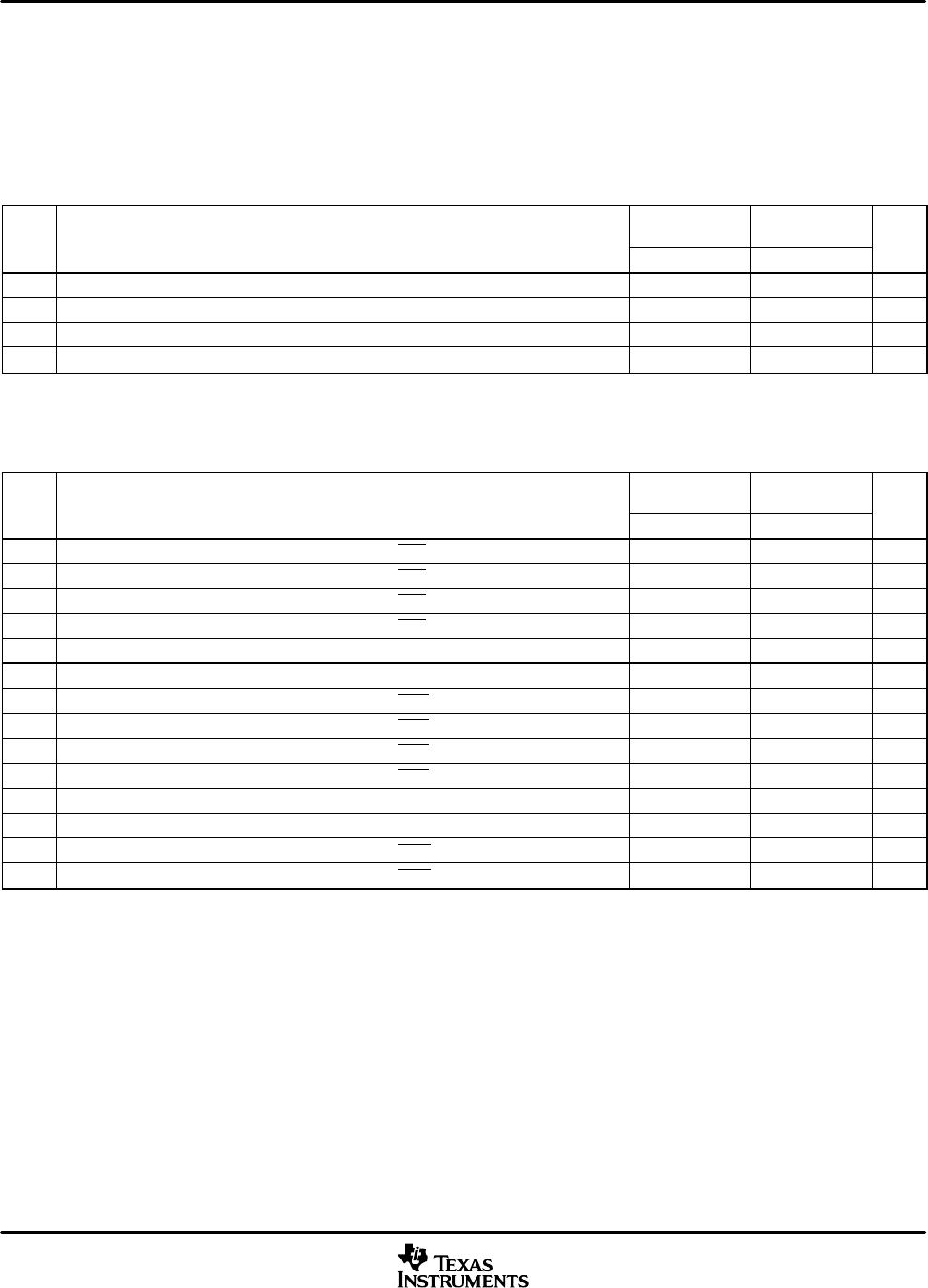
Table 5−7 and Table 5−8 assume testing over recommended operating conditions (see Figure 5−6 and
Figure 5−7).
Table 5−7. Asynchronous Memory Cycle Timing Requirements
NO.
CV
DD
= 1.2 V
CV
DD
= 1.35 V
CV
DD
= 1.6 V
UNIT
NO.
MIN MAX MIN MAX
UNIT
M1 t
su(DV-COH)
Setup time, read data valid before CLKOUT high
6 5 ns
M2 t
h(COH-DV)
Hold time, read data valid after CLKOUT high 0 0 ns
M3 t
su(ARDY-COH)
Setup time, ARDY valid before CLKOUT high
10 7 ns
M4 t
h(COH-ARDY)
Hold time, ARDY valid after CLKOUT high 0 0 ns
To ensure data setup time, simply program the strobe width wide enough. ARDY is internally synchronized. If ARDY does meet setup or hold
time, it may be recognized in the current cycle or the next cycle. Thus, ARDY can be an asynchronous input.
Table 5−8. Asynchronous Memory Cycle Switching Characteristics
NO.
PARAMETER
CV
DD
= 1.2 V
CV
DD
= 1.35 V
CV
DD
= 1.6 V
UNIT
NO.
PARAMETER
MIN MAX MIN MAX
UNIT
M5 t
d(COH-CEV)
Delay time, CLKOUT high to CEx valid −2 4 −2 4 ns
M6 t
d(COH-CEIV)
Delay time, CLKOUT high to CEx invalid −2 4 −2 4 ns
M7 t
d(COH-BEV)
Delay time, CLKOUT high to BEx valid 4 4 ns
M8 t
d(COH-BEIV)
Delay time, CLKOUT high to BEx invalid −2 −2 ns
M9 t
d(COH-AV)
Delay time, CLKOUT high to address valid 4 4 ns
M10 t
d(COH-AIV)
Delay time, CLKOUT high to address invalid −2 −2 ns
M11 t
d(COH-AOEV)
Delay time, CLKOUT high to AOE valid −2 4 −2 4 ns
M12 t
d(COH-AOEIV)
Delay time, CLKOUT high to AOE invalid −2 4 −2 4 ns
M13 t
d(COH-AREV)
Delay time, CLKOUT high to ARE valid −2 4 −2 4 ns
M14 t
d(COH-AREIV)
Delay time, CLKOUT high to ARE invalid −2 4 −2 4 ns
M15 t
d(COH-DV)
Delay time, CLKOUT high to data valid 4 4 ns
M16 t
d(COH-DIV)
Delay time, CLKOUT high to data invalid −2 −2 ns
M17 t
d(COH-AWEV)
Delay time, CLKOUT high to AWE valid −2 4 −2 4 ns
M18 t
d(COH-AWEIV)
Delay time, CLKOUT high to AWE invalid −2 4 −2 4 ns
PREVIOUS2425262728293031323334353637NEXT