Freelance Electronics Components Distributor
Closed Dec 25th-26th
800-300-1968
We Stock Hard to Find Parts

TMS320VC5509APGE

Part # TMS320VC5509APGE
Description FIXED POINT DIGITAL SIGNAL PROCESSOR -DSP, 32 BIT, 200MHZ
Category IC
Availability Out of Stock
Qty 0
Qty Price
1 + $22.73692


Technical Document


DISCLAIMER: The information provided herein is solely for informational purposes. Customers must be aware of the suitability of this product for their application, and consider that variable factors such as Manufacturer, Product Category, Date Codes, Pictures and Descriptions may differ from available inventory.

Electrical Specifications
88
November 2002 − Revised January 2005SPRS205D
5.6 Clock Options
The frequency of the reference clock provided at the X2/CLKIN pin can be divided by a factor of two or four
or multiplied by one of several values to generate the internal machine cycle.
5.6.1 Internal System Oscillator With External Crystal
The internal oscillator is always enabled following a device reset. The oscillator requires an external crystal
connected across the X1 and X2/CLKIN pins. If the internal oscillator is not used, an external clock source
must be applied to the X2/CLKIN pin and the X1 pin should be left unconnected. Since the internal oscillator
can be used as a clock source to the PLLs, the crystal oscillation frequency can be multiplied to generate the
CPU clock and USB clock, if desired.
The crystal should be in fundamental-mode operation, and parallel resonant, with a maximum effective series
resistance (ESR) specified in Table 5−1. The connection of the required circuit is shown in Figure 5−2. Under
some conditions, all the components shown are not required. The capacitors, C
1
and C
2
, should be chosen
such that the equation below is satisfied. C
L
in the equation is the load specified for the crystal that is also
specified in Table 5−1.
C
L
+
C
1
C
2
(C
1
) C
2
)
X2/CLKIN
X1
C1 C2
Crystal
R
S
Figure 5−2. Internal System Oscillator With External Crystal
Table 5−1. Recommended Crystal Parameters
FREQUENCY RANGE (MHz) MAX ESR () TYP C
LOAD
(pF) MAX C
SHUNT
(pF) R
S
()
20−15 20 10 7 0
15−12 30 16 7 0
12−10 40 16 7 100
10−8 60 18 7 470
8−6 80 18 7 1.5k
6−5 80 18 7 2.2k
Although the recommended ESR presented in Table 5−1 is maximum, theoretically a crystal with a lower
maximum ESR might seem to meet the requirement. It is recommended that crystals which meet the
maximum ESR specification in Table 5−1 are used.
Electrical Specifications
89
November 2002 − Revised January 2005 SPRS205D
5.6.2 Layout Considerations
Since parasitic capacitance, inductance and resistance can be significant in any circuit, good PC board layout
practices should always be observed when planning trace routing to the discrete components used in the
oscillator circuit. Specifically, the crystal and the associated discrete components should be located as close
to the DSP as physically possible. Also, X1 and X2/CLKIN traces should be separated as soon as possible
after routing away from the DSP to minimize parasitic capacitance between them, and a ground trace should
be run between these two signal lines. This also helps to minimize stray capacitance between these two
signals.
Electrical Specifications
90
November 2002 − Revised January 2005SPRS205D
5.6.3 Clock Generation in Bypass Mode (DPLL Disabled)
The frequency of the reference clock provided at the X2/CLKIN pin can be divided by a factor of one, two, or
four to generate the internal CPU clock cycle. The divide factor (D) is set in the BYPASS_DIV field of the clock
mode register. The contents of this field only affect clock generation while the device is in bypass mode. In
this mode, the digital phase-locked loop (DPLL) clock synthesis is disabled.
Table 5−2 and Table 5−3 assume testing over recommended operating conditions and H = 0.5t
c(CO)
(see
Figure 5−3).
Table 5−2. CLKIN Timing Requirements
NO.
CV
DD
= 1.2 V
CV
DD
= 1.35 V
CV
DD
= 1.6 V
UNIT
MIN MAX
C1 t
c(CI)
Cycle time, X2/CLKIN 20 400
ns
C2 t
f(CI)
Fall time, X2/CLKIN 4 ns
C3 t
r(CI)
Rise time, X2/CLKIN 4 ns
C10 t
w(CIL)
Pulse duration, CLKIN low 6 ns
C11 t
w(CIH)
Pulse duration, CLKIN high 6 ns
This device utilizes a fully static design and therefore can operate with t
c(CI)
approaching . If an external crystal is used, the X2/CLKIN cycle
time is limited by the crystal frequency range listed in Table 5−1.
Table 5−3. CLKOUT Switching Characteristics
NO.
PARAMETER
CV
DD
= 1.2 V
CV
DD
= 1.35 V
CV
DD
= 1.6 V
UNIT
MIN TYP MAX
C4 t
c(CO)
Cycle time, CLKOUT 20
D*t
c(CI)
§
1600
ns
C5 t
d(CI-CO)
Delay time, X2/CLKIN high to CLKOUT high/low 5 15 25 ns
C6 t
f(CO)
Fall time, CLKOUT 1 ns
C7 t
r(CO)
Rise time, CLKOUT 1 ns
C8 t
w(COL)
Pulse duration, CLKOUT low H − 1 H + 1 ns
C9 t
w(COH)
Pulse duration, CLKOUT high H − 1 H + 1 ns
This device utilizes a fully static design and therefore can operate with t
c(CO)
approaching . If an external crystal is used, the X2/CLKIN cycle
time is limited by the crystal frequency range listed in Table 5−1.
It is recommended that the DPLL synthesised clocking option be used to obtain maximum operating frequency.
§
D = 1/(PLL Bypass Divider)
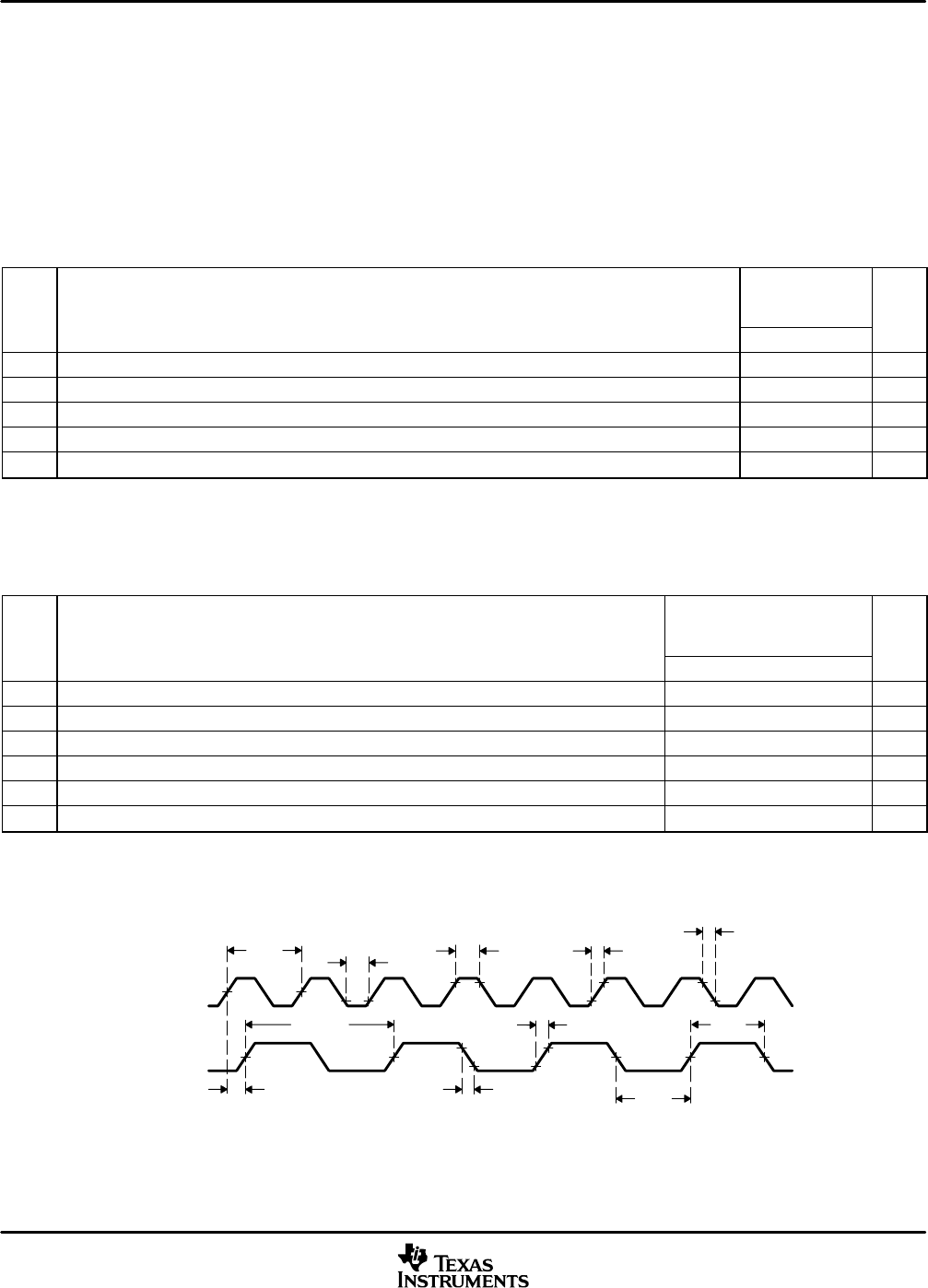
C3
C2
C1
C4
C5
C7
C6
C8
C9
X2/CLKIN
CLKOUT
C10
C11
NOTE A: The relationship of X2/CLKIN to CLKOUT depends on the PLL bypass divide factor chosen for the CLKMD register. The waveform
relationship shown in Figure 5−3 is intended to illustrate the timing parameters based on CLKOUT = 1/2(CLKIN) configuration.
Figure 5−3. Bypass Mode Clock Timings
PREVIOUS2324252627282930313233343536NEXT