Electrical Specifications
87
November 2002 − Revised January 2005 SPRS205D
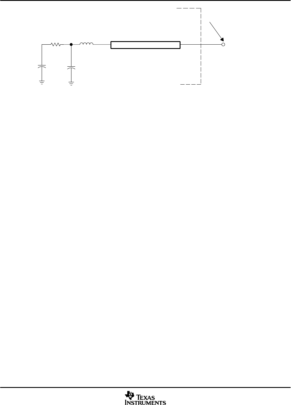
Transmission Line
4.0 pF 1.85 pF
Z0 = 50 Ω
(see note)
Tester Pin Electronics
Data Manual Timing Reference Point
Output
Under
Test
NOTE: The data manual provides timing at the device pin. For output timing analysis, the tester pin electronics and its transmission line effects
must be taken into account. A transmission line with a delay of 2 ns or longer can be used to produce the desired transmission line effect.
The transmission line is intended as a load only. It is not necessary to add or subtract the transmission line delay (2 ns or longer) from
the data manual timings.
42 Ω 3.5 nH
Device Pin
(see note)
Input requirements in this data manual are tested with an input slew rate of < 4 Volts per nanosecond (4 V/ns) at the device
pin.
Figure 5−1. 3.3-V Test Load Circuit
5.4 ESD Performance
ESD stress levels were performed in compliance with the following JEDEC standards with the results indicated
below:
• Charged Device Model (CDM), based on JEDEC Specification JESD22-C101, passed at ±500 V
• Human Body Model (HBM), based on JEDEC Specification JESD22-A114, passed at ±1500 V
NOTE:
According to industry research publications, ESD-CDM testing results show better correlation
to manufacturing line and field failure rates than ESD-HBM testing. 500-V CDM is commonly
considered as a safe passing level.
5.5 Timing Parameter Symbology
Timing parameter symbols used in the timing requirements and switching characteristics tables are created
in accordance with JEDEC Standard 100. To shorten the symbols, some of the pin names and other related
terminology have been abbreviated as follows:
Lowercase subscripts and their meanings: Letters and symbols and their meanings:
a access time H High
c cycle time (period) L Low
d delay time V Valid
dis disable time Z High-impedance
en enable time
f fall time
h hold time
r rise time
su setup time
t transition time
v valid time
w pulse duration (width)
X Unknown, changing, or don’t care level


