Freelance Electronics Components Distributor
Closed Dec 25th-26th
800-300-1968
We Stock Hard to Find Parts

TMS320VC5509APGE

Part # TMS320VC5509APGE
Description FIXED POINT DIGITAL SIGNAL PROCESSOR -DSP, 32 BIT, 200MHZ
Category IC
Availability Out of Stock
Qty 0
Qty Price
1 + $22.73692


Technical Document


DISCLAIMER: The information provided herein is solely for informational purposes. Customers must be aware of the suitability of this product for their application, and consider that variable factors such as Manufacturer, Product Category, Date Codes, Pictures and Descriptions may differ from available inventory.

Support
79
November 2002 − Revised January 2005 SPRS205D
4.4 TMS320VC5509A Device Nomenclature
PREFIX
TMS 320 VC 5509A GHH
TMX = Experimental device
TMP = Prototype device
TMS = Qualified device
SMJ = MIL-STD-883C
SM = High Rel (non-883C)
DEVICE FAMILY
320 = TMS320 family
TECHNOLOGY
PACKAGE TYPE
GHH = 179-terminal plastic BGA
ZHH = 179-terminal plastic BGA (lead-free)
PGE = 144-pin plastic LQFP
VC = Dual-Supply CMOS
DEVICE
55x DSP:
5509A
No silicon revision marked on the package indicates earlier (TMX or TMP) silicon. See the TMS320VC5509A Digital Signal Processor
Silicon Errata (literature number SPRZ200) to identify TMX or TMP silicon revision.
BGA = Ball Grid Array
LQFP = Low-Profile Quad Flatpack
(10)
DEVICE SILICON REVISION
10 = Revision 1.0
11 = Revision 1.1
Figure 4−1. Device Nomenclature for the TMS320VC5509A
Electrical Specifications
80
November 2002 − Revised January 2005SPRS205D
5 Electrical Specifications
This section provides the absolute maximum ratings and the recommended operating conditions for the
TMS320VC5509A DSP.
All electrical and switching characteristics in this data manual are valid over the recommended operating
conditions unless otherwise specified.
5.1 Absolute Maximum Ratings
The list of absolute maximum ratings are specified over operating case temperature. Stresses beyond those
listed under “absolute maximum ratings” may cause permanent damage to the device. These are stress
ratings only, and functional operation of the device at these or any other conditions beyond those indicated
under Section 5.2 is not implied. Exposure to absolute-maximum-rated conditions for extended periods may
affect device reliability. All voltage values are with respect to V
SS
. Figure 5−1 provides the test load circuit
values for a 3.3-V I/O.
Supply voltage I/O range, DV
DD
− 0.3 V to 4.0 V. . . . . . . . . . . . . . . . . . . . . . . . . . . . . . . . . . . . . . . . . . . . . . . . .
Supply voltage core range, CV
DD
− 0.3 V to 2.0 V. . . . . . . . . . . . . . . . . . . . . . . . . . . . . . . . . . . . . . . . . . . . . . . . .
Input voltage range, V
I
− 0.3 V to 4.5 V. . . . . . . . . . . . . . . . . . . . . . . . . . . . . . . . . . . . . . . . . . . . . . . . . . . . . . . . .
Output voltage range, V
O
− 0.3 V to 4.5 V. . . . . . . . . . . . . . . . . . . . . . . . . . . . . . . . . . . . . . . . . . . . . . . . . . . . . . . .
Operating case temperature range, T
C
40°C to 85°C. . . . . . . . . . . . . . . . . . . . . . . . . . . . . . . . . . . . . . . . . . . .
Storage temperature range T
stg
55°C to 150°C. . . . . . . . . . . . . . . . . . . . . . . . . . . . . . . . . . . . . . . . . . . . . . . . . .
Electrical Specifications
81
November 2002 − Revised January 2005 SPRS205D
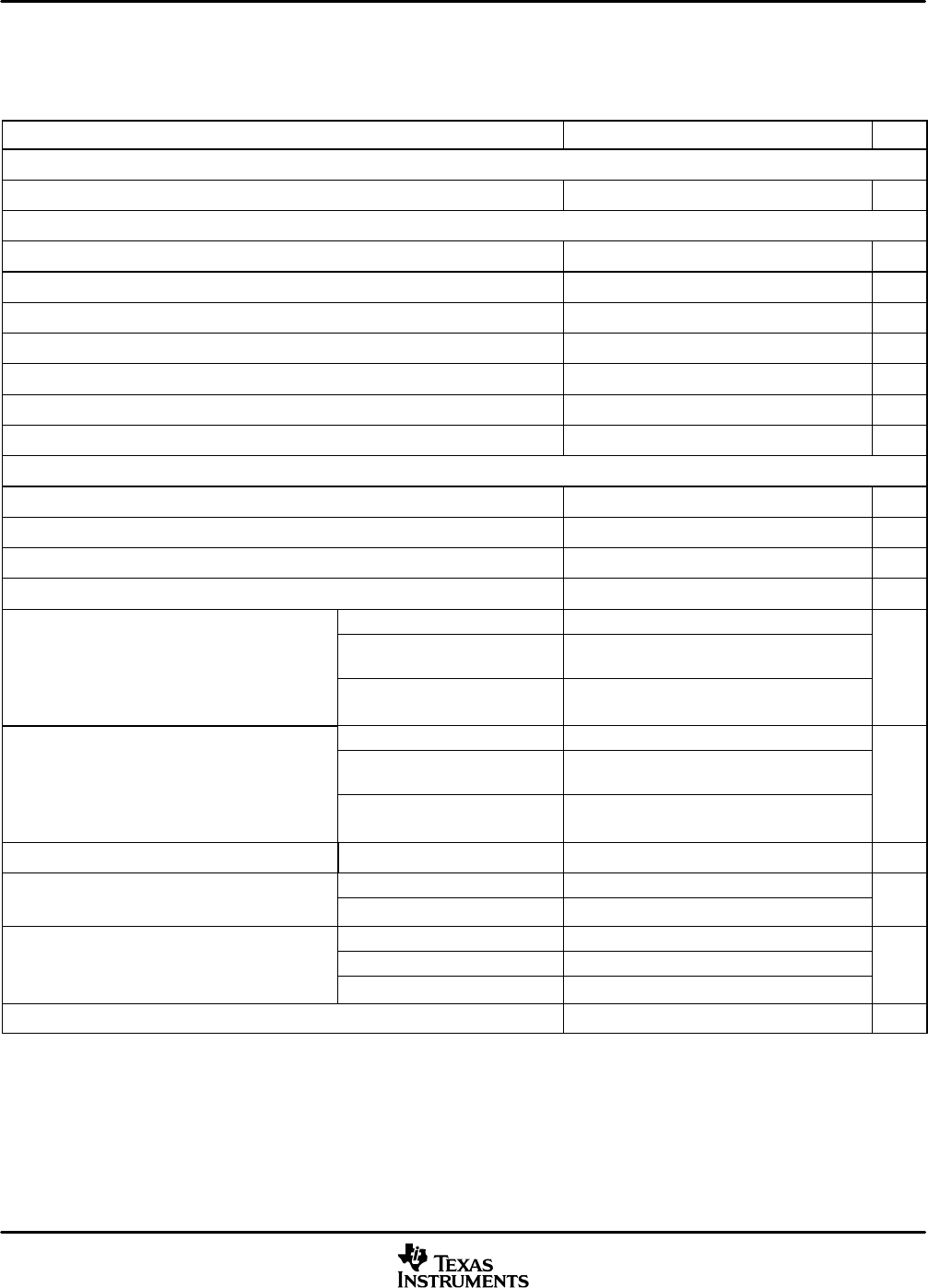
5.2 Recommended Operating Conditions
5.2.1 Recommended Operating Conditions for CV
DD
= 1.2 V (108 MHz)
MIN NOM MAX UNIT
Core
CV
DD
Device supply voltage 1.14 1.2 1.26 V
Peripherals
RCV
DD
RTC module supply voltage, core 1.14 1.2 1.26 V
RDV
DD
RTC module supply voltage, I/O (RTCINX1 and RTCINX2) 1.14 1.2 1.26 V
USBPLLV
DD
USBPLL supply voltage
1.14 1.2 1.26 V
USBV
DD
USB module supply voltage, I/O (DP, DN, and PU) 3 3.3 3.6 V
DV
DD
Device supply voltage, I/O (except DP, DN, PU, SDA, SCL)
2.7 3.3 3.6 V
ADV
DD
A/D module digital supply voltage 2.7 3.3 3.6 V
AV
DD
A/D module analog supply voltage 2.7 3.3 3.6 V
Grounds
V
SS
Supply voltage, GND, I/O, and core 0 V
ADV
SS
Supply voltage, GND, A/D module, digital 0 V
AV
SS
Supply voltage, GND, A/D module, analog 0 V
USBPLLV
SS
Supply voltage, GND, USBPLL 0 V
DN and DP
§
2.0
V
IH
High-level input voltage, I/O
SDA & SCL: V
DD
related input
levels
0.7*DV
DD
DV
DD
(max) +0.5
V
V
IH
High-level input voltage, I/O
All other inputs
(including hysteresis inputs)
2.0 DV
DD
+ 0.3
V
DN and DP
§
0.8
V
IL
Low-level input voltage, I/O
SDA &SCL: V
DD
related input
levels
−0.5 0.3 * DV
DD
V
V
IL
Low-level input voltage, I/O
All other inputs
(including hysteresis inputs)
−0.3 0.8
V
V
hys
Hysteresis level Inputs with hysteresis only 0.1*DV
DD
V
I
OH
High-level output current
DN and DP
§
(V
OH
= 2.45 V) −17.0
mA
I
OH
High-level output current
All other outputs −4
mA
DN and DP
§
(V
OL
= 0.36 V) 17.0
I
OL
Low-level output current
SDA and SCL
3
mA
I
OL
Low-level output current
All other outputs 4
mA
T
C
Operating case temperature −40 85
_C
USB PLL is susceptible to power supply ripple. The maximum allowable supply ripple is 1% for 1 Hz to 5 kHz; 1.5% for 5 kHz to 10 MHz; 3%
for 10 MHz to 100 MHz, and less than 5% for 100 MHz or greater.
The I
2
C pins SDA and SCL do not feature fail-safe I/O buffers. These pins could potentially draw current when the device is powered down.
Due to the fact that different voltage devices can be connected to the I
2
C bus, the level of logic 0 (low) and logic 1 (high) are not fixed and
depends on the associated V
DD
.
§
USB I/O pins DP and DN can tolerate a short circuit at D+ and D− to 0 V or 5 V, as long as the recommended series resistors (see Figure 5−42)
are connected between the D+ and DP (package), and the D− and DN (package). Do not apply a short circuit to the USB I/O pins DP and DN
in absence of the series resistors.
PREVIOUS2021222324252627282930313233NEXT