Functional Overview
70
November 2002 − Revised January 2005SPRS205D
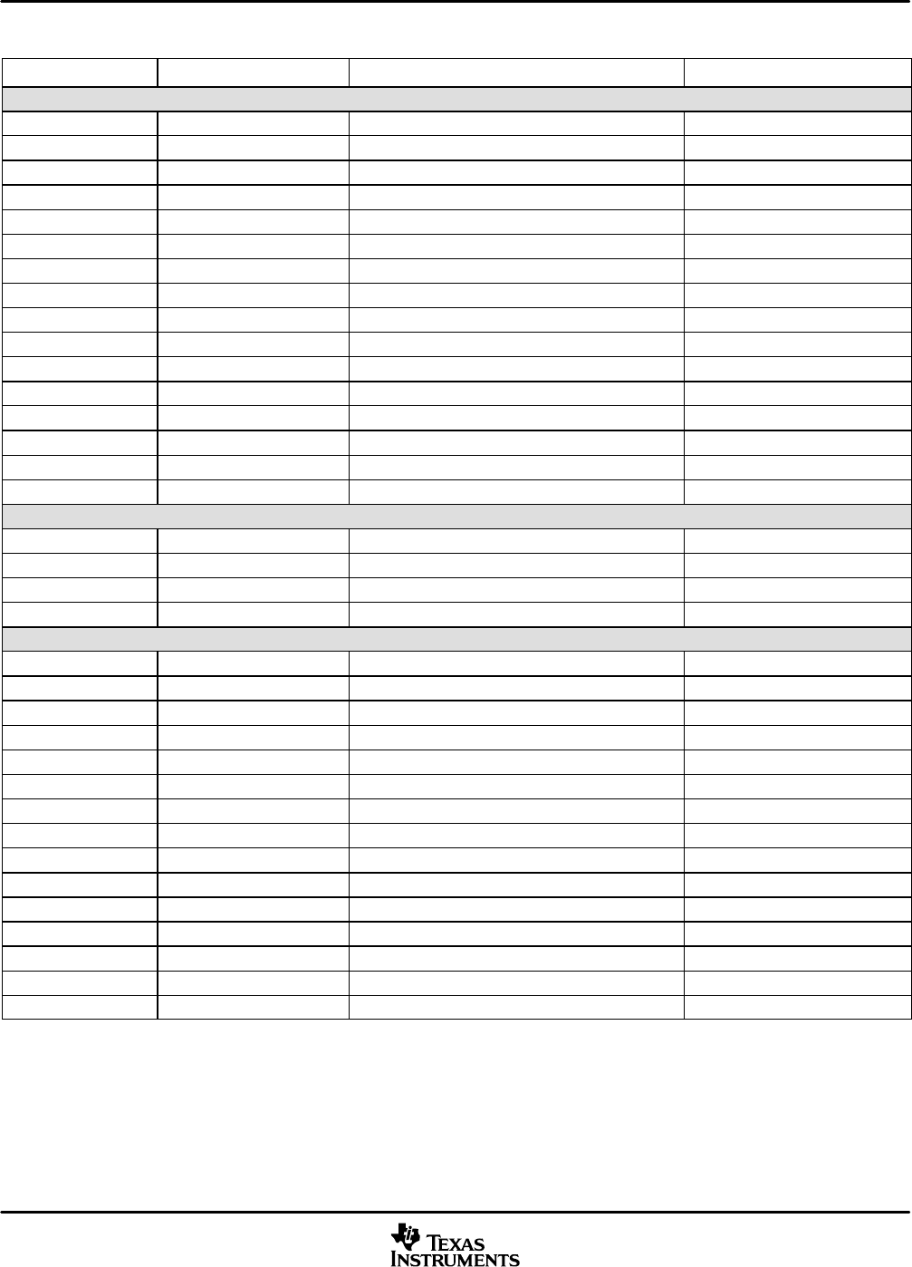
Table 3−37. USB Module Registers
WORD ADDRESS REGISTER NAME DESCRIPTION
RESET VALUE
†
DMA CONTEXTS
0x5800 Reserved
0x5808 DMAC_O1 Output Endpoint 1 DMA Context Register Undefined
0x5810 DMAC_O2 Output Endpoint 2 DMA Context Register Undefined
0x5818 DMAC_O3 Output Endpoint 3 DMA Context Register Undefined
0x5820 DMAC_O4 Output Endpoint 4 DMA Context Register Undefined
0x5828 DMAC_O5 Output Endpoint 5 DMA Context Register Undefined
0x5830 DMAC_O6 Output Endpoint 6 DMA Context Register Undefined
0x5838 DMAC_O7 Output Endpoint 7 DMA Context Register Undefined
0x5840 Reserved
0x5848 DMAC_I1 Input Endpoint 1 DMA Context Register Undefined
0x5850 DMAC_I2 Input Endpoint 2 DMA Context Register Undefined
0x5858 DMAC_I3 Input Endpoint 3 DMA Context Register Undefined
0x5860 DMAC_I4 Input Endpoint 4 DMA Context Register Undefined
0x5868 DMAC_I5 Input Endpoint 5 DMA Context Register Undefined
0x5870 DMAC_I6 Input Endpoint 6 DMA Context Register Undefined
0x5878 DMAC_I7 Input Endpoint 7 DMA Context Register Undefined
DATA BUFFER
0x5880 Data Buffers Contains X/Y data buffers for endpoints 1 – 7 Undefined
0x6680 OEB_0 Output Endpoint 0 Buffer Undefined
0x66C0 IEB_0 Input Endpoint 0 Buffer Undefined
0x6700 SUP_0 Setup Packet for Endpoint 0 Undefined
ENDPOINT DESCRIPTOR BLOCKS
0x6708 OEDB_1 Output Endpoint 1 Descriptor Register Block Undefined
0x6710 OEDB_2 Output Endpoint 2 Descriptor Register Block Undefined
0x6718 OEDB_3 Output Endpoint 3 Descriptor Register Block Undefined
0x6720 OEDB_4 Output Endpoint 4 Descriptor Register Block Undefined
0x6728 OEDB_5 Output Endpoint 5 Descriptor Register Block Undefined
0x6730 OEDB_6 Output Endpoint 6 Descriptor Register Block Undefined
0x6738 OEDB_7 Output Endpoint 7 Descriptor Register Block Undefined
0x6740 Reserved
0x6748 IEDB_1 Input Endpoint 1 Descriptor Register Block Undefined
0x6750 IEDB_2 Input Endpoint 2 Descriptor Register Block Undefined
0x6758 IEDB_3 Input Endpoint 3 Descriptor Register Block Undefined
0x6760 IEDB_4 Input Endpoint 4 Descriptor Register Block Undefined
0x6768 IEDB_5 Input Endpoint 5 Descriptor Register Block Undefined
0x6770 IEDB_6 Input Endpoint 6 Descriptor Register Block Undefined
0x6778 IEDB_7 Input Endpoint 7 Descriptor Register Block Undefined
†
Hardware reset; x denotes a “don’t care.”
NOTE: The USB module must be brought out of reset by setting bit 2 of the USB Idle Control and Status Register before any USB module register
read or write attempt.


