Freelance Electronics Components Distributor
Closed Dec 25th-26th
800-300-1968
We Stock Hard to Find Parts

TMS320VC5509APGE

Part # TMS320VC5509APGE
Description FIXED POINT DIGITAL SIGNAL PROCESSOR -DSP, 32 BIT, 200MHZ
Category IC
Availability Out of Stock
Qty 0
Qty Price
1 + $22.73692


Technical Document


DISCLAIMER: The information provided herein is solely for informational purposes. Customers must be aware of the suitability of this product for their application, and consider that variable factors such as Manufacturer, Product Category, Date Codes, Pictures and Descriptions may differ from available inventory.

Functional Overview
61
November 2002 − Revised January 2005 SPRS205D
Table 3−24. DMA Configuration Registers (Continued)
PORT ADDRESS
(WORD)
RESET VALUE
DESCRIPTIONREGISTER NAME
CHANNEL #4 REGISTERS
0x0C80 DMA_CSDP4 DMA Channel 4 Source Destination
Parameters Register
0000 0000 0000 0000
0x0C81 DMA_CCR4[15:0] DMA Channel 4 Control Register 0000 0000 0000 0000
0x0C82 DMA_CICR4[5:0] DMA Channel 4 Interrupt Control Register xxxx xxxx xx00 0011
0x0C83 DMA_CSR4[6:0] DMA Channel 4 Status Register xxxx xxxx xx00 0000
0x0C84 DMA_CSSA_L4 DMA Channel 4 Source Start Address Register
(lower bits)
Undefined
0x0C85 DMA_CSSA_U4 DMA Channel 4 Source Start Address Register
(upper bits)
Undefined
0x0C86 DMA_CDSA_L4 DMA Channel 4 Source Destination Address Register
(lower bits)
Undefined
0x0C87 DMA_CDSA_U4 DMA Channel 4 Source Destination Address Register
(upper bits)
Undefined
0x0C88 DMA_CEN4 DMA Channel 4 Element Number Register Undefined
0x0C89 DMA_CFN4 DMA Channel 4 Frame Number Register Undefined
0x0C8A DMA_CFI4/
DMA_CSFI4
DMA Channel 4 Frame Index Register/
DMA Channel 4 Source Frame Index Register
Undefined
0x0C8B DMA_CEI4/
DMA_CSEI4
§
DMA Channel 4 Element Index Register/
DMA Channel 4 Source Element Index Register
§
Undefined
0x0C8C DMA_CSAC4 DMA Channel 4 Source Address Counter Undefined
0x0C8D DMA_CDAC4 DMA Channel 4 Destination Address Counter Undefined
0x0C8E DMA_CDEI4 DMA Channel 4 Destination Element Index Register Undefined
0x0C8F DMA_CDFI4 DMA Channel 4 Destination Frame Index Register Undefined
Hardware reset: x denotes a “don’t care.”
On the TMS320VC5509, the channel frame index applies to both source and destination and this register behaves as DMA_CFIn. On the
TMS320VC5509A, DMA_CSFIn and DMA_CDFIn provide separate source and destination frame indexing. The 5509A can be programmed
for software compatibility with the 5509 through the Software Compatibility Register (DMA_GSCR).
§
On the TMS320VC5509, the channel element index applies to both source and destination and this register behaves as DMA_CEIn. On the
TMS320VC5509A, DMA_CSEIn and DMA_CDEIn provide separate source and destination frame indexing. The 5509A can be programmed
for software compatibility with the 5509 through the Software Compatibility Register (DMA_GSCR).
Functional Overview
62
November 2002 − Revised January 2005SPRS205D
Table 3−24. DMA Configuration Registers (Continued)
PORT ADDRESS
(WORD)
RESET VALUE
DESCRIPTIONREGISTER NAME
CHANNEL #5 REGISTERS
0x0CA0 DMA_CSDP5 DMA Channel 5 Source Destination
Parameters Register
0000 0000 0000 0000
0x0CA1 DMA_CCR5[15:0] DMA Channel 5 Control Register 0000 0000 0000 0000
0x0CA2 DMA_CICR5[5:0] DMA Channel 5 Interrupt Control Register xxxx xxxx xx00 0011
0x0CA3 DMA_CSR5[6:0] DMA Channel 5 Status Register xxxx xxxx xx00 0000
0x0CA4 DMA_CSSA_L5 DMA Channel 5 Source Start Address Register
(lower bits)
Undefined
0x0CA5 DMA_CSSA_U5 DMA Channel 5 Source Start Address Register
(upper bits)
Undefined
0x0CA6 DMA_CDSA_L5 DMA Channel 5 Source Destination Address Register
(lower bits)
Undefined
0x0CA7 DMA_CDSA_U5 DMA Channel 5 Source Destination Address Register
(upper bits)
Undefined
0x0CA8 DMA_CEN5 DMA Channel 5 Element Number Register Undefined
0x0CA9 DMA_CFN5 DMA Channel 5 Frame Number Register Undefined
0x0CAA DMA_CFI5/
DMA_CSFI5
DMA Channel 5 Frame Index Register/
DMA Channel 5 Source Frame Index Register
Undefined
0x0CAB DMA_CEI5/
DMA_CSEI5
§
DMA Channel 5 Element Index Register/
DMA Channel 5 Source Element Index Register
§
Undefined
0x0CAC DMA_CSAC5 DMA Channel 5 Source Address Counter Undefined
0x0CAD DMA_CDAC5 DMA Channel 5 Destination Address Counter Undefined
0x0CAE DMA_CDEI5 DMA Channel 5 Destination Element Index Register Undefined
0x0CAF DMA_CDFI5 DMA Channel 5 Destination Frame Index Register Undefined
Hardware reset: x denotes a “don’t care.”
On the TMS320VC5509, the channel frame index applies to both source and destination and this register behaves as DMA_CFIn. On the
TMS320VC5509A, DMA_CSFIn and DMA_CDFIn provide separate source and destination frame indexing. The 5509A can be programmed
for software compatibility with the 5509 through the Software Compatibility Register (DMA_GSCR).
§
On the TMS320VC5509, the channel element index applies to both source and destination and this register behaves as DMA_CEIn. On the
TMS320VC5509A, DMA_CSEIn and DMA_CDEIn provide separate source and destination frame indexing. The 5509A can be programmed
for software compatibility with the 5509 through the Software Compatibility Register (DMA_GSCR).
Functional Overview
63
November 2002 − Revised January 2005 SPRS205D
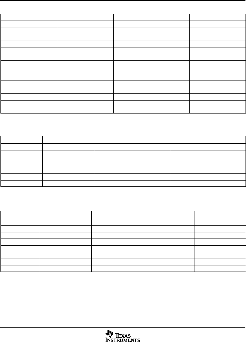
Table 3−25. Real-Time Clock Registers
WORD ADDRESS REGISTER NAME DESCRIPTION RESET VALUE
0x1800 RTCSEC Seconds Register 0000 0000 0000 0000
0x1801 RTCSECA Seconds Alarm Register 0000 0000 0000 0000
0x1802 RTCMIN Minutes Register 0000 0000 0000 0000
0x1803 RTCMINA Minutes Alarm Register 0000 0000 0000 0000
0x1804 RTCHOUR Hours Register 0000 0000 0000 0000
0x1805 RTCHOURA Hours Alarm Register 0000 0000 0000 0000
0x1806 RTCDAYW Day of the Week Register 0000 0000 0000 0000
0x1807 RTCDAYM Day of the Month (date) Register 0000 0000 0000 0000
0x1808 RTCMONTH Month Register 0000 0000 0000 0000
0x1809 RTCYEAR Year Register 0000 0000 0000 0000
0x180A RTCPINTR Periodic Interrupt Selection Register 0000 0000 0000 0000
0x180B RTCINTEN Interrupt Enable Register 0000 0000 1000 0000
0x180C RTCINTFL Interrupt Flag Register 0000 0000 0000 0000
0x180D−0x1BFF Reserved
Hardware reset; x denotes a “don’t care.”
Table 3−26. Clock Generator
WORD ADDRESS REGISTER NAME DESCRIPTION
RESET VALUE
0x1C00 CLKMD[14:0] Clock Mode Register 0010 0000 0000 0010 DIV1 mode
0x1E00
USBDPLL[14:0]
USB DPLL Control Register
If non-USB boot mode:
0010 0000 0000 0110 DIV2 mode
0x1E00
USBDPLL[14:0]
USB DPLL Control Register
If USB boot mode:
0010 0010 0001 0011 PLL MULT4 mode
0x1E80 USBPLLSEL[2:0] USB PLL Selection Register 0000 0000 0000 0100
0x1F00 USBAPLL[15:0] USB APLL Control Register 0000 0000 0000 0000
Hardware reset; x denotes a “don’t care.”
DPLL is the power-up default USB clock source.
Table 3−27. Timers
WORD ADDRESS REGISTER NAME DESCRIPTION
RESET VALUE
0x1000 TIM0[15:0] Timer Count Register, Timer #0 1111 1111 1111 1111
0x1001 PRD0[15:0] Period Register, Timer #0 1111 1111 1111 1111
0x1002 TCR0[15:0] Timer Control Register, Timer #0 0000 0000 0001 0000
0x1003 PRSC0[15:0] Timer Prescaler Register, Timer #0 xxxx 0000 xxxx 0000
0x2400 TIM1[15:0] Timer Count Register, Timer #1 1111 1111 1111 1111
0x2401 PRD1[15:0] Period Register, Timer #1 1111 1111 1111 1111
0x2402 TCR1[15:0] Timer Control Register, Timer #1 0000 0000 0001 0000
0x2403 PRSC1[15:0] Timer Prescaler Register, Timer #1 xxxx 0000 xxxx 0000
Hardware reset; x denotes a “don’t care.”
PREVIOUS1415161718192021222324252627NEXT