Functional Overview
52
November 2002 − Revised January 2005SPRS205D
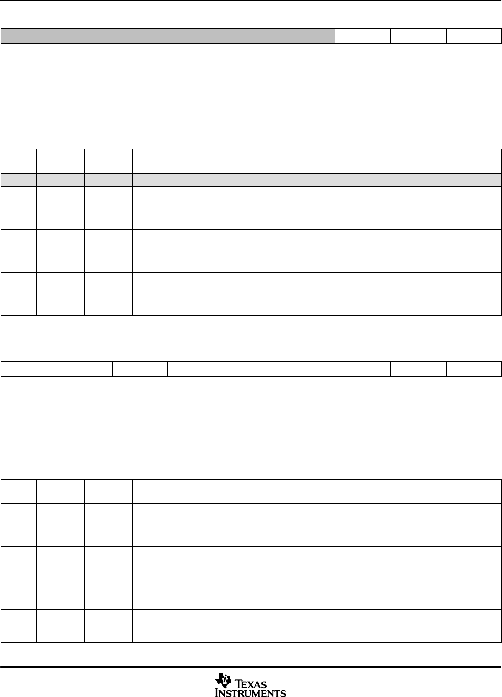
15 3210
Reserved DPLLSTAT APLLSTAT PLLSEL
R, 0000 0000 0000 0 R, 1 R, 0 R/W, 0
LEGEND: R = Read, W = Write, n = value after reset
Figure 3−18. USB PLL Selection and Status Register Bit Layout
Table 3−18. USB PLL Selection and Status Register Bit Functions
BIT
NO.
BIT
NAME
RESET
VALUE
FUNCTION
15−3 Reserved 0 Reserved bits. Always write 0.
2 DPLLSTAT 1
Status bit indicating if the DPLL is the source for the USB module clock.
DPLLSTAT = 0 The DPLL is not the USB module clock source.
DPLLSTAT = 1 The DPLL is the USB module clock source.
1 APLLSTAT 0
Status bit indicating if the APLL is the source for the USB module clock.
APLLSTAT = 0 The APLL is not the USB module clock source.
APLLSTAT = 1 The APLL is the USB module clock source.
0 PLLSEL 0
USB module clock source selection bit.
PLLSEL = 0 DPLL is selected as USB module clock source.
PLLSEL = 1 APLL is selected as USB module clock source.
15 12 11 10 3 2 1 0
MULT DIV COUNT ON MODE STAT
R/W, 0000 R/W, 0 R, 0000 0000 R/W, 0 R/W, 0 R, 0
LEGEND: R = Read, W = Write, n = value after reset
Figure 3−19. USB APLL Clock Mode Register Bit Layout
Table 3−19. USB APLL Clock Mode Register Bit Functions
BIT
NO.
BIT
NAME
RESET
VALUE
FUNCTION
15−12 MULT 0
PLL Multiply Factor K. Multiply Factor K, combined with DIV and MODE, determines the final PLL output
clock frequency.
K = MULT[3:0] + 1
11 DIV 0
PLL Divide Factor (D) selection bit for PLL multiply mode operation. DIV, combined with K and MODE,
determines the final PLL output clock frequency. When the PLL is operating in multiply mode:
DIV = 0 PLL Divide Factor D = 1
DIV = 1 PLL Divide Factor D = 2 if K is odd
PLL Divide Factor D = 4 if K is even
10−3 COUNT 0
8-bit counter for PLL lock timer. When the MODE bit is set to 1, the COUNT field starts decrementing by 1
at the rate of CLKIN/16. When COUNT decrements to 0, the STAT bit is set to 1 and the PLL enabled clock
is sourced to the USB module.


