Freelance Electronics Components Distributor
Closed Dec 25th-26th
800-300-1968
We Stock Hard to Find Parts

TMS320VC5509APGE

Part # TMS320VC5509APGE
Description FIXED POINT DIGITAL SIGNAL PROCESSOR -DSP, 32 BIT, 200MHZ
Category IC
Availability Out of Stock
Qty 0
Qty Price
1 + $22.73692


Technical Document


DISCLAIMER: The information provided herein is solely for informational purposes. Customers must be aware of the suitability of this product for their application, and consider that variable factors such as Manufacturer, Product Category, Date Codes, Pictures and Descriptions may differ from available inventory.

Functional Overview
49
November 2002 − Revised January 2005 SPRS205D
3.6.3 EHPI General-Purpose I/O
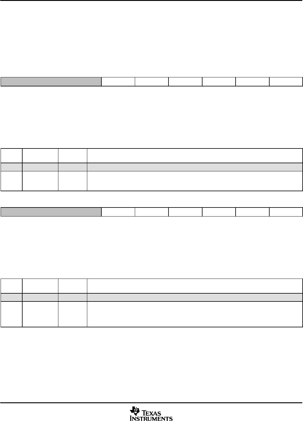
Six control lines of the External Parallel Bus can also be set as general-purpose I/O when the Parallel Port
Mode bit field of the External Bus Selection Register is set to Nonmultiplexed EHPI (10) or Multiplexed EHPI
mode (11). These pins are controlled by three registers: the enable register, EHPIGPIOEN, determines if the
pins serve as GPIO or address (Figure 3−13); the direction register, EHPIGPIODIR, determines if the GPIO
enabled pin is an input or output (Figure 3−14); and the data register, EHPIGPIODATA, determines the logic
states of the pins in GPIO mode (Figure 3−15).
15 6543210
Reserved GPIOEN13 GPIOEN12 GPIOEN11 GPIOEN10 GPIOEN9 GPIOEN8
R, 0000 0000 00 R/W, 0 R/W, 0 R/W, 0 R/W, 0 R/W, 0 R/W, 0
LEGEND: R = Read, W = Write, n = value after reset
Figure 3−13. EHPI GPIO Enable Register (EHPIGPIOEN) Bit Layout
Table 3−14. EHPI GPIO Enable Register (EHPIGPIOEN) Bit Functions
BIT
NO.
BIT
NAME
RESET
VALUE
FUNCTION
15−6 Reserved 0 Reserved
5−0
GPIOEN13−
GPIOEN8
0
Enable or disable GPIO function of EHPI Control Bus.
GPIOENx = 0 GPIO function of GPIOx line is disabled
GPIOENx = 1 GPIO function of GPIOx line is enabled
15 6543210
Reserved GPIODIR13 GPIODIR12 GPIODIR11 GPIODIR10 GPIODIR9 GPIODIR8
R, 0000 0000 00 R/W, 0 R/W, 0 R/W, 0 R/W, 0 R/W, 0 R/W, 0
LEGEND: R = Read, W = Write, n = value after reset
Figure 3−14. EHPI GPIO Direction Register (EHPIGPIODIR) Bit Layout
Table 3−15. EHPI GPIO Direction Register (EHPIGPIODIR) Bit Functions
BIT
NO.
BIT
NAME
RESET
VALUE
FUNCTION
15−6 Reserved 0 Reserved
5−0
GPIODIR13−
GPIODIR8
0
Data direction bits that configure the EHPI Control Bus configured as I/O pins as either input or output
pins.
GPIODIRx = 0 Configure corresponding pin as an input.
GPIODIRx = 1 Configure corresponding pin as an output.
Functional Overview
50
November 2002 − Revised January 2005SPRS205D
15 6543210
Reserved GPIOD13 GPIOD12 GPIOD11 GPIOD10 GPIOD9 GPIOD8
R, 0000 0000 00 R/W, 0 R/W, 0 R/W, 0 R/W, 0 R/W, 0 R/W, 0
LEGEND: R = Read, W = Write, n = value after reset
Figure 3−15. EHPI GPIO Data Register (EHPIGPIODATA) Bit Layout
Table 3−16. EHPI GPIO Data Register (EHPIGPIODATA) Bit Functions
BIT
NO.
BIT
NAME
RESET
VALUE
FUNCTION
15−6 Reserved 0 Reserved
5−0
GPIOD13−
GPIOD8
0
Data bits that are used to control the level of the EHPI Control Bus configured as I/O output pins, and to
monitor the level of the EHPI Control Bus configured as I/O input pins.
If GPIODIRn = 0, then:
GPIODx = 0 Corresponding I/O pin is read as a low.
GPIODx = 1 Corresponding I/O pin is read as a high.
If GPIODIRn = 1, then:
GPIODx = 0 Set corresponding I/O pin to low.
GPIODx = 1 Set corresponding I/O pin to high.
Functional Overview
51
November 2002 − Revised January 2005 SPRS205D
3.7 System Register
The system register (SYSR) provides control over certain device-specific functions. The register is located
at port address 07FDh.
15 8
Reserved
7320
Reserved CLKDIV
R/W
LEGEND: R = Read, W = Write, n = value after reset
Figure 3−16. System Register Bit Locations
Table 3−17. System Register Bit Fields
BIT
NUMBER NAME
15−3 Reserved These bits are reserved and are unaffected by writes.
2−0
CLKDIV CLKOUT Divide Factor. Allows the clock present on the CLKOUT pin to be a divided-down version
of the internal CPU clock. This field does not affect the programming of the PLL.
CLKDIV 000 = CLKOUT represents the CPU clock divided by 1
CLKDIV 001 = CLKOUT represents the CPU clock divided by 2
CLKDIV 010 = CLKOUT represents the CPU clock divided by 4
CLKDIV 011 = CLKOUT represents the CPU clock divided by 6
CLKDIV 100 = CLKOUT represents the CPU clock divided by 8
CLKDIV 101 = CLKOUT represents the CPU clock divided by 10
CLKDIV 110 = CLKOUT represents the CPU clock divided by 12
CLKDIV 111 = CLKOUT represents the CPU clock divided by 14
3.8 USB Clock Generation
The USB module can be clocked from either an Analog Phase-Locked Loop (APLL) or a Digital Phase-Locked
Loop (DPLL). The APLL is the recommended USB clock source due to better noise tolerance and less
long-term jitter than the DPLL. To maintain the backward compatibility, the DPLL is the power-up default clock
source for the USB module.
USB
APLL
DPLL
USB
1
0
USB Module Clock
(48.0 MHz)
PLLSEL
CLKIN
Figure 3−17. USB Clock Generation
PREVIOUS1011121314151617181920212223NEXT